
Camera chip surface black spot compensation method

A compensation method and camera technology, applied in the direction of image communication, TV, color TV components, etc., to achieve the effect of accurate compensation calculation

Active Publication Date: 2022-06-10
JIANGXI HOLITECH TECH
View PDF11 Cites 0 Cited by
  • Summary
  • Abstract
  • Description
  • Claims
  • Application Information

AI Technical Summary

Problems solved by technology

However, this method only compensates for each channel, and does not judge whether a single pixel is a black point, that is, it does not judge whether each pixel itself is an abnormal pixel, and the compensation for the pixel is not accurate

Method used


Image

  • Camera chip surface black spot compensation method
  • Camera chip surface black spot compensation method
  • Camera chip surface black spot compensation method

Examples


Embodiment Construction

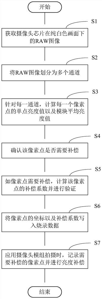
[0029] The present invention is applied to an electronic device with a camera, such as a smart phone, a tablet computer, etc., and the electronic device is provided with a camera chip. see figure 1 , the method of the present invention first executes step S1 to acquire a RAW image of the camera chip under a pure white screen. For example, the camera module is lit under the G4C light source board to save the RAW image under the pure white screen. If there is no abnormality in the camera chip, that is, there is no black spot, the image obtained under the pure white screen is as follows: figure 2 shown. If there is an abnormal pixel in the camera chip, that is, the pixel is a black spot, a black spot will be formed in the image, such as image 3 shown. The area where the black spots are formed is the area where the abnormal pixels are located. The present invention mainly compensates for the abnormal pixels to eliminate the black pixels.

[0030] After acquiring the RAW ima...


PUM


Abstract

The invention provides a camera chip surface black spot compensation method, which comprises the following steps: acquiring a RAW image of a camera module in a pure white picture, and splitting the RAW image into a plurality of channels; for each channel, calculating a single-point brightness value of each pixel point; calculating a module average brightness value of a module taking each pixel point as a center, determining whether the brightness value of the pixel point needs to be compensated or not according to the single-point brightness value of the pixel point and the module average brightness value, and calculating a compensation coefficient of the pixel point if the brightness value of the pixel point needs to be compensated; verifying the compensation coefficient; writing the position of the pixel point needing to be compensated and the compensation coefficient of the pixel point into chip burning data; when the electronic equipment uses the camera module to take a picture, the position of a pixel point needing to be compensated is recorded, the compensation coefficient corresponding to the pixel point is obtained, and the compensation coefficient is used for compensating the brightness value of the pixel point. According to the invention, black spots of the camera chip can be effectively compensated, and the yield of the camera chip is improved.

Description

technical field [0001] The invention relates to the technical field of compensation processing of a camera chip, in particular to a method for compensating black spots on the surface of a camera chip. Background technique [0002] Many existing intelligent electronic devices have the function of image capture, such as smartphones, tablet computers, driving recorders, etc. are all equipped with camera devices, and the camera devices are usually equipped with a camera chip to capture images through the camera chip. However, affected by the production process of the camera chip, it is inevitable to form black spots on the surface of the camera chip. With the development of smart phone technology, the quality requirements for camera chips are getting higher and higher, and the requirements for black spots on the surface of camera chips are becoming more and more stringent. For example, very strict requirements are required for the number of black spots on the surface of camera c...

Claims


Application Information

Patent Timeline
Patent Type & Authority Applications(China)
IPC IPC(8): H04N5/235H04N9/77
CPCH04N9/77H04N23/71
Inventor 吴毅
Owner JIANGXI HOLITECH TECH
Learn More