Thin-film encapsulation structure and organic light-emitting diode display thereof

A light-emitting diode and thin-film packaging technology, which is applied in the direction of organic semiconductor devices, electric solid-state devices, semiconductor devices, etc., can solve problems such as the inability to reflect the density of inorganic thin-film layers and water-repellent film quality, the inability to optimize, and the monitoring of coating quality. Achieve the effect of reducing non-luminous dark spots

Inactive Publication Date: 2015-05-20
AU OPTRONICS CORP
View PDF0 Cites 20 Cited by
  • Summary
  • Abstract
  • Description
  • Claims
  • Application Information

AI Technical Summary

Problems solved by technology

Furthermore, the common quantitative coating quality only monitors the uniformity and thickness of the coating, which cannot reflect the density and water-repelling film quality of the inorganic thin film layer, and cannot optimize and monitor the coating quality, resulting in lower pass rates and lower water resistance. Decrease, causing water, oxygen and other organic substances to easily pass through the inorganic thin film layer to attack OLED and cause black spots that do not emit light

Method used


Image

  • Thin-film encapsulation structure and organic light-emitting diode display thereof
  • Thin-film encapsulation structure and organic light-emitting diode display thereof
  • Thin-film encapsulation structure and organic light-emitting diode display thereof

Examples


Embodiment Construction

[0037] In order to make the technical content disclosed in this application more detailed and complete, reference may be made to the drawings and the following various specific embodiments of the present invention, and the same symbols in the drawings represent the same or similar components. However, those skilled in the art should understand that the examples provided below are not intended to limit the scope of the present invention. In addition, the drawings are only for schematic illustration and are not drawn according to their original scale.

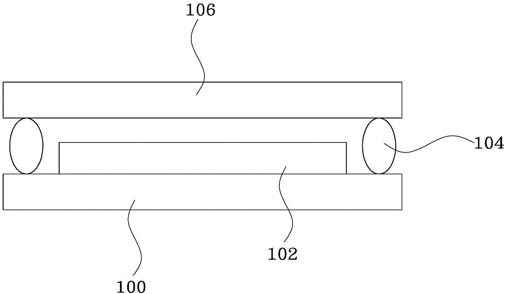
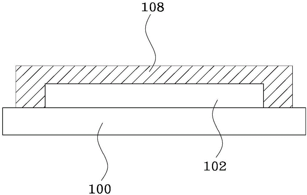
[0038] Figure 1A A schematic diagram showing a packaging structure of an organic light-emitting diode based on adhesive bonding in the prior art.

[0039] refer to Figure 1A, the conventional OLED display includes a first glass substrate (first glass substrate) 100 , an OLED 102 , a sealing layer (sealant) 104 and a second glass substrate (second glass substrate) 106 . Here, the second glass substrate 106 may also be referred ...


PUM


Abstract

The invention discloses a thin-film encapsulation structure and an organic light-emitting diode display thereof. The thin-film encapsulation structure comprises an organic light-emitting diode, a first inorganic thin-film layer, organic thin-film layers and a second inorganic thin-film layer, wherein the first inorganic thin-film layer has first Young modulus; the first inorganic thin-film layer is located above the organic light-emitting diode and covers the organic light-emitting diode; the organic thin-film layers are stacked above the first inorganic thin-film layer; the second inorganic thin-film layer has second Young modulus; the second inorganic thin-film layer is located above the organic thin-film layers; the first Young modulus is greater than the second Young modulus. Compared with the prior art, the Young modulus of one inorganic thin-film layer close to the organic light-emitting diode is higher than that of another inorganic thin-film layer far away from the organic light-emitting diode, so that the quantitative standard of the compactness of the inorganic thin-film layers can be solved; the condition that the organic light-emitting diode cannot be damaged by vapor or organic matters on the upper layer is ensured; in addition, the lightless black spots on reaction of the organic matters caused by processing plasma can also be reduced by the thin-film encapsulation structure.

Description

technical field [0001] The invention relates to a packaging technology of an organic light emitting diode, in particular to a thin film packaging structure for the organic light emitting diode and an organic light emitting diode display including the thin film packaging structure. Background technique [0002] Among the existing flat-panel displays, organic light emitting diode (OLED) displays can provide wide viewing angles, good contrast ratio and fast response speed, and have higher brightness and lower Therefore, it has gradually received widespread attention and favor from people. Currently, flexible AMOLED (Active Matrix OLED) displays are one of the research and development priorities of major domestic and foreign manufacturers and research institutes. Compared with ordinary displays, flexible AMOLED has the characteristics of light weight, flexibility, easy storage, and portability. [0003] In a nutshell, the flexible AMOLED mainly includes a flexible substrate, a...

Claims


Application Information

Patent Timeline
Patent Type & Authority Applications(China)
IPC IPC(8): H01L51/52H01L51/56H01L27/32
CPCH10K59/12H10K50/84H10K2102/311H10K71/00
Inventor 宋大豪杨介宏萧如正李孟庭
Owner AU OPTRONICS CORP
Why Eureka
Try Eureka