

Manufacturing process of circuit pattern of outer-layer flexible rigid-flex circuit board
A technology of circuit board circuit and rigid-flex combination, which is applied in multilayer circuit manufacturing, printed circuit manufacturing, printed circuit, etc., to achieve batch production, solve process defects, and improve the overall industry technology effect
Active Publication Date: 2022-06-10
信丰迅捷兴电路科技有限公司
View PDF5 Cites 1 Cited by
- Summary
- Abstract
- Description
- Claims
- Application Information
AI Technical Summary
Problems solved by technology
Therefore, the present invention belongs to the technology of the printed circuit board industry. To be precise, it is a process method to solve the problem of poor dry film lamination caused by the depression of the soft board of the rigid-flex circuit board in the outer layer structure.
Method used
View moreImage
Smart ImageViewing Examples

Examples
Embodiment Construction
Login to View More PUM
| Property | Measurement | Unit |
|---|---|---|
| angle | aaaaa | aaaaa |
| thickness | aaaaa | aaaaa |
| thickness | aaaaa | aaaaa |
Abstract
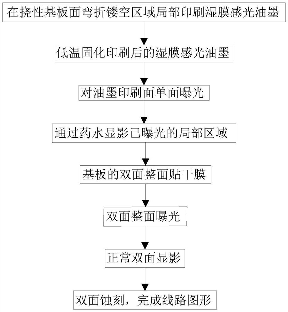
A process for manufacturing a circuit pattern of an outer-layer flexible rigid-flex circuit board comprises the following steps of: printing ink, namely locally printing wet film photosensitive ink in a bent hollow area of a flexible substrate surface; curing the printed wet film photosensitive ink at low temperature; performing single-side exposure on the ink printing surface; developing the exposed local area through liquid medicine; dry films are pasted on the whole double surfaces of the substrate; double-sided whole-surface exposure is performed, a wet film is exposed, and a developing area is not repeatedly exposed any more, so that developing and film removal are facilitated; normal double-sided development; and finally finishing the circuit pattern. Through the wet film and dry film process method, the phenomenon that the dry film cannot be compacted and broken due to the fact that the outer layer flexible substrate is sunken due to the fact that the prepreg is hollowed out is solved; according to the wet ink printing process method, a concave area can be completely coated, a dry film is pasted for secondary exposure after exposure and development of a circuit pattern, meanwhile, exposure avoids a wet film area, and the technological process of combining the dry film with the wet film is achieved.
Description
technical field [0001] The present invention relates to the field of printed circuit boards, in particular to a manufacturing process of circuit graphics of an outer layer flexible rigid-flex circuit board, through the process of adding wet film and dry film to solve the problem of cracking of the dry film caused by the depression of the outer layer substrate , applied to rigid-flex circuit boards and all types of circuit boards in which the flexible substrate is recessed in the outer layer and the outer layer surface. . Background technique [0002] With the precision and miniaturization of electronic devices, the advantages of multi-dimensional installation and arbitrary layer interconnection of rigid-flex circuit boards are being used in more and more fields; at present, the production of rigid-flex circuit The flexible bending area of the prepreg is hollowed out, and then the flexible substrate and the rigid substrate are stacked by pressing and bonding, and finally t...
Claims
Login to View More Application Information
Patent Timeline
 Patent Type & Authority Applications(China)
IPC IPC(8): H05K3/06H05K3/46
CPCH05K3/06H05K3/4691H05K2203/1476
Inventor 陈定成宋波
Owner 信丰迅捷兴电路科技有限公司