Check patentability & draft patents in minutes with Patsnap Eureka AI!

Optical waveguide device

一种光波导、波长的技术,应用在光束引导装置、光波导光导、光导等方向,能够解决降低分辨率、不能消除缺陷、增加花费等问题

Inactive Publication Date: 2006-11-15
GIFU UNIVERSITY
View PDF0 Cites 0 Cited by
  • Summary
  • Abstract
  • Description
  • Claims
  • Application Information

AI Technical Summary

Problems solved by technology

However, if a light source with light intensity is used to increase the intensity of near-field light, it will increase the cost
On the other hand, if you increase the size of the end opening, the light is spread over a wider area and the resolution is reduced
Therefore, neither case can eliminate the drawbacks in practical application

Method used


Image

  • Optical waveguide device
  • Optical waveguide device
  • Optical waveguide device

Examples


Embodiment Construction

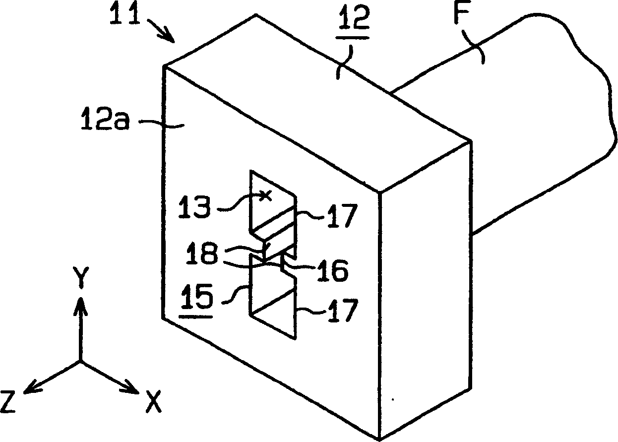
[0058] will now refer to Figure 1 to Figure 8 , describes the optical waveguide device 11 according to the first embodiment, which is an optical probe.

[0059] Such as figure 1 As shown, the optical waveguide device (optical probe) 11 of this embodiment includes: a main body 12, which is a rectangular metal plate. The body 12 is made of a dielectric having a negative real part of the relative complex permittivity. That is, body 12 is made of a negative dielectric (plasmon activation medium). In this embodiment, the wavelength of transmitted light is 488nm (nanometer), and the body 12 is made of silver (Ag), wherein the real part of the relative complex permittivity is -7.38. The relative complex permittivity of the dielectric is represented by the ratio of the permittivity of the dielectric to the permittivity in vacuum.

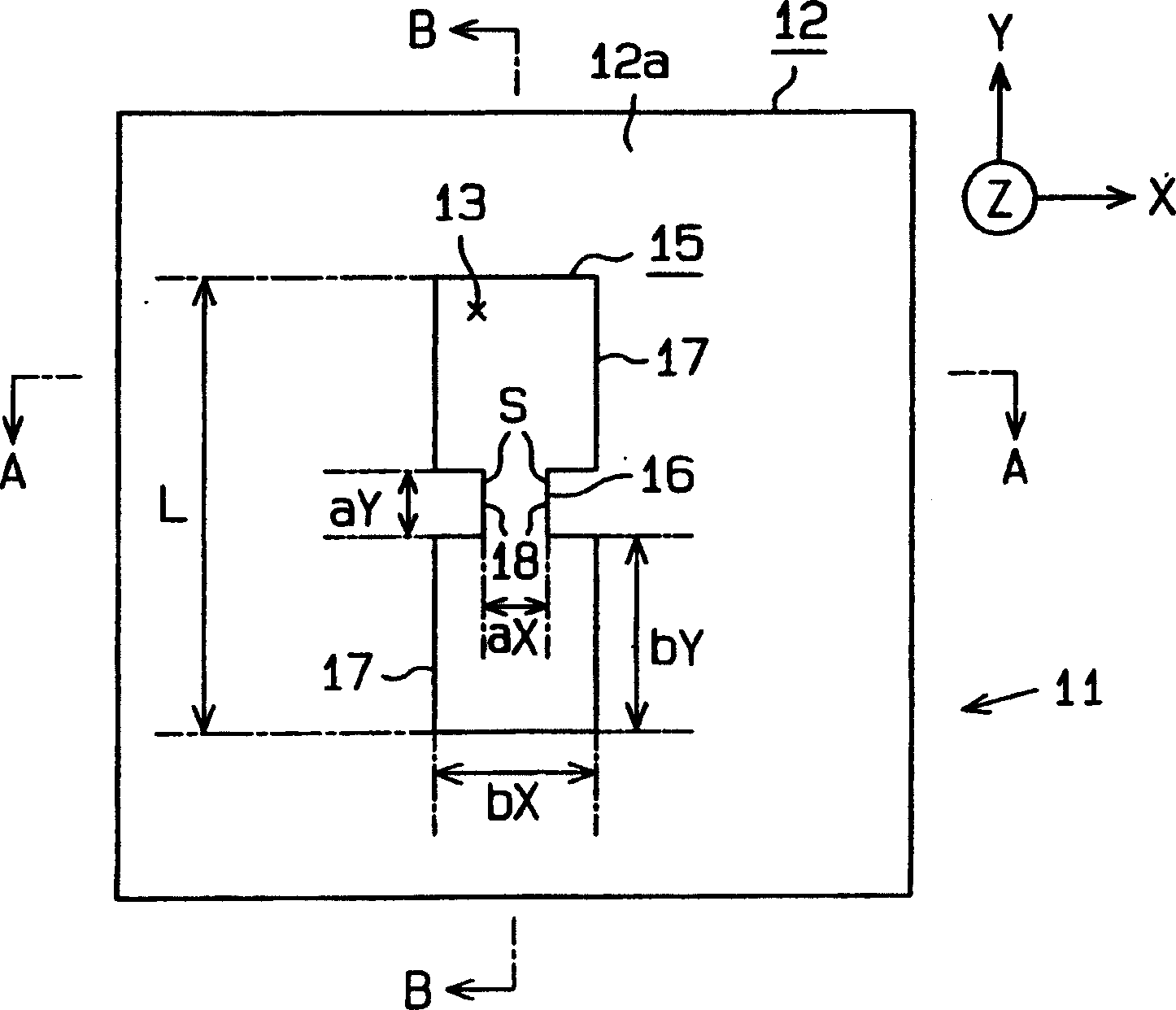
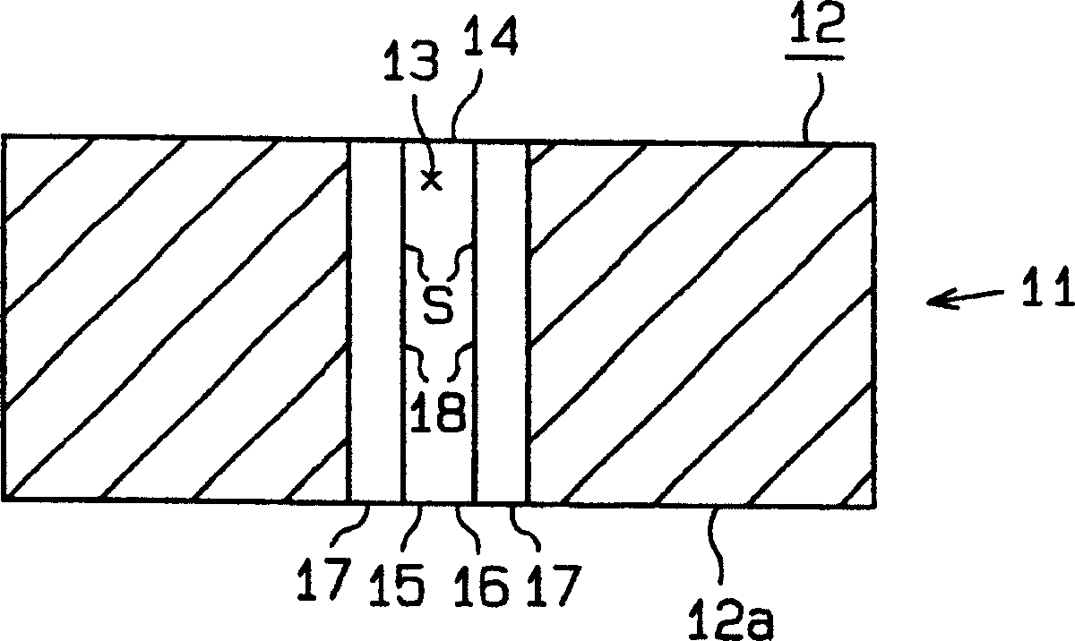
[0060] Such asfigure 1 , 3(a), and 3(b), an optical waveguide 13 for transmitting light is formed on the main body 12 through the thickness direction....


PUM

PropertyMeasurementUnit
wavelengthaaaaaaaaaa
sizeaaaaaaaaaa
sizeaaaaaaaaaa

Abstract

An optical waveguide device that increases the intensity of light transmitted through a reduced-cost optical waveguide without enlarging the area of ​​light. An optical waveguide arrangement according to the invention comprises: an optical waveguide, and a defining surface for the first optical waveguide. Define the surface to be made of a plasmon-activated medium. The defining surface includes: a pair of inner portions facing each other along a direction perpendicular to the light transmission direction. The distance between the inner parts is less than half the wavelength of light transmitted through the optical waveguide.

Description

technical field [0001] The present invention relates to an optical waveguide suitable for scanning near-field optical microscopes and optical data recorders. Background technique [0002] In recent years, as a technology that can optically process light in a region smaller than the wavelength of light (visible light: 0.4 to 0.8 micrometers), technology using near-field light (light that reaches a region shorter than the wavelength of light) has attracted extreme attention. Big attention. For example, in the field of scanning near-field optical microscopy, an optical probe composed of an optical fiber having minute openings is used as an optical waveguide. The size of the opening is smaller than the wavelength of light. When observing a minute area on the surface of a sample, the minute opening of the optical probe is positioned very close to the area, and the light field (near field) appearing outside the opening comes into contact with the surface of the sample. Then, a ...

Claims


Application Information

Patent Timeline
Patent Type & Authority Patents(China)
IPC IPC(8): G02B6/10G01Q60/18G01Q60/22G01Q80/00G02B6/00G02B6/122G02B6/24G11B7/135H01L21/027
CPCG01Q60/22G02B6/10G02B6/1226G02B6/241B82Y20/00B82Y35/00
Inventor 田中嘉津夫田中雅宏
Owner GIFU UNIVERSITY
Features
  • R&D
  • Intellectual Property
  • Life Sciences
  • Materials
  • Tech Scout
  • Unparalleled Data Quality
  • Higher Quality Content
  • 60% Fewer Hallucinations
Learn More