Matrix, Liquid crystal display device and electronic instrument
A technology of liquid crystal display devices and substrates, which can be used in the direction of instruments, identification devices, static indicators, etc., and can solve problems such as discharge
- Summary
- Abstract
- Description
- Claims
- Application Information
AI Technical Summary
Problems solved by technology
Method used
Image

Examples
Embodiment approach 1
[0059] Next, Embodiment 1 of a substrate and a liquid crystal display device in the present invention will be described with reference to the drawings.
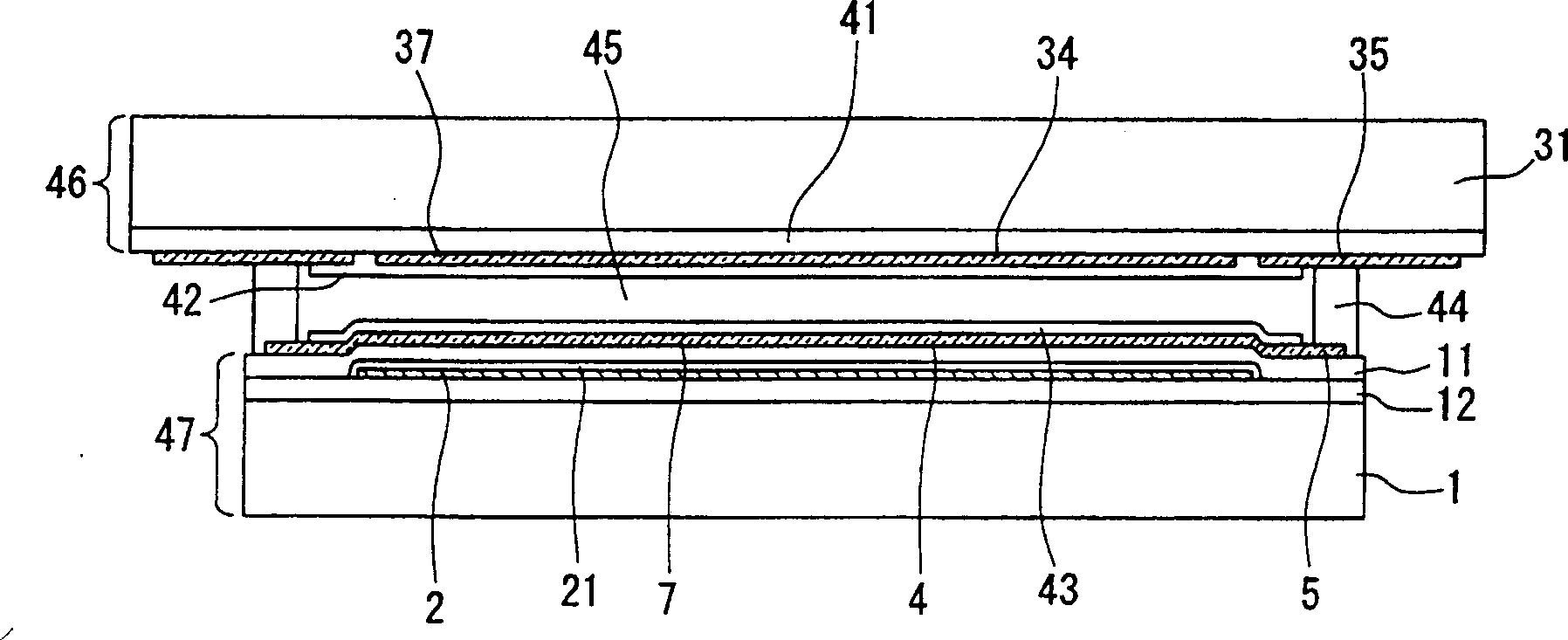
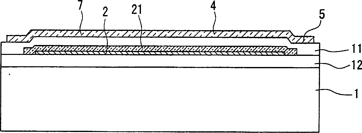
[0060] figure 1 It is a cross-sectional view showing the liquid crystal display device in this embodiment. figure 2 yes means figure 1 A cross-sectional view of a common substrate in a liquid crystal display device. image 3 is a plan view showing the same common substrate. Figure 4 yes image 3 magnified top view of .
[0061] The liquid crystal display device in this embodiment is a reflective simple matrix liquid crystal display device. In the figure, reference numeral 1 denotes a first substrate, 2 denotes a reflective film, and 3 denotes a display area.
[0062] In this liquid crystal display device, basically, a liquid crystal layer 45 made of STN (super-twisted nematic) liquid crystal or the like is sandwiched between a pair of substrates 1, 31 made of glass substrates or the like.
[0063] Such as figure 1...
Embodiment approach 2
[0093] Next, Embodiment 2 of the substrate and the liquid crystal display device in the present invention will be described with reference to the drawings.
[0094] In this embodiment, with Figure 1 ~ Figure 4 The difference between the illustrated first embodiment lies in the arrangement of the electrode 7 with respect to the reflective film 2 . The same symbols are used for other constituent elements, and explanations thereof are omitted.
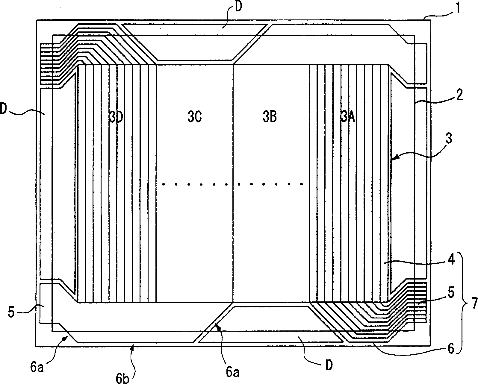
[0095] Figure 5 It is a plan view showing the common substrate in the liquid crystal display device of the present embodiment.
[0096] In the common substrate 47 of this embodiment, the configuration of the reflective film 2 relative to the underlying substrate 1 is the same as image 3 , Figure 4 The shown implementation 1 is slightly different, as Figure 5 As shown, in each of the electrodes 7, 7, the lead wirings 6', 6' completely overlap the reflective film 2.
[0097] In short, the portions of the electrodes 7, 7 that do n...
Embodiment approach 3
[0104] Next, Embodiment 3 of the substrate and the liquid crystal display device in the present invention will be described with reference to the drawings.
[0105] In this embodiment, with Figure 1 ~ Figure 4 The difference between the illustrated first embodiment lies in the arrangement of the reflective film 2 with respect to the underlying substrate 1 . The same symbols are used for other constituent elements, and explanations thereof are omitted.
[0106] Image 6 It is a plan view showing the common substrate in the liquid crystal display device of the present embodiment.
[0107] In the common substrate 47 of this embodiment, it is set that the reflective film 2 has approximately the same area as the underlying substrate 1, such as Image 6 As shown, each electrode 7, 7 completely overlaps with the reflective film 2.
[0108] That is, it is set so that there is no portion that does not overlap the reflective film 2 among the electrodes 7, 7 .
[0109] Moreover, th...
PUM
 Abstract
Description
Claims
Application Information
 - R&D Engineer
- R&D Manager
- IP Professional
- Industry Leading Data Capabilities
- Powerful AI technology
- Patent DNA Extraction
Browse by: Latest US Patents, China's latest patents, Technical Efficacy Thesaurus, Application Domain, Technology Topic.
© 2024 PatSnap. All rights reserved.Legal|Privacy policy|Modern Slavery Act Transparency Statement|Sitemap