Check patentability & draft patents in minutes with Patsnap Eureka AI!

Camera module and mfg. method thereof

A manufacturing method and camera technology, which are applied in multilayer circuit manufacturing, semiconductor/solid-state device manufacturing, image communication, etc., can solve the problems of complex installation structure and increased cost of camera modules.

Inactive Publication Date: 2004-02-18
SANYO ELECTRIC CO LTD
View PDF1 Cites 3 Cited by
  • Summary
  • Abstract
  • Description
  • Claims
  • Application Information

AI Technical Summary

Problems solved by technology

[0012] First, the chip part 103, the back chip part 104, the lens 105, the lens barrel 106, the lens holder 107, and the CCD 102 are necessary constituent elements, but it is difficult to provide miniaturization, thinning, and weight reduction only by these constituent elements. camera module
[0013] Second, when the existing camera module 100 is installed inside the casing of devices such as digital cameras, the camera module 100 has a problem of complicated installation structure because its two sides are not formed flat.
[0015] Fourth, there is a tendency for the lead-out electrodes of ICs to have more leads and narrow pitches. In order to follow this trend, the mounting substrate 101 must have a multilayer wiring structure of about four layers, which leads to an increase in the cost of the camera module.

Method used


Image

  • Camera module and mfg. method thereof
  • Camera module and mfg. method thereof
  • Camera module and mfg. method thereof

Examples


Embodiment Construction

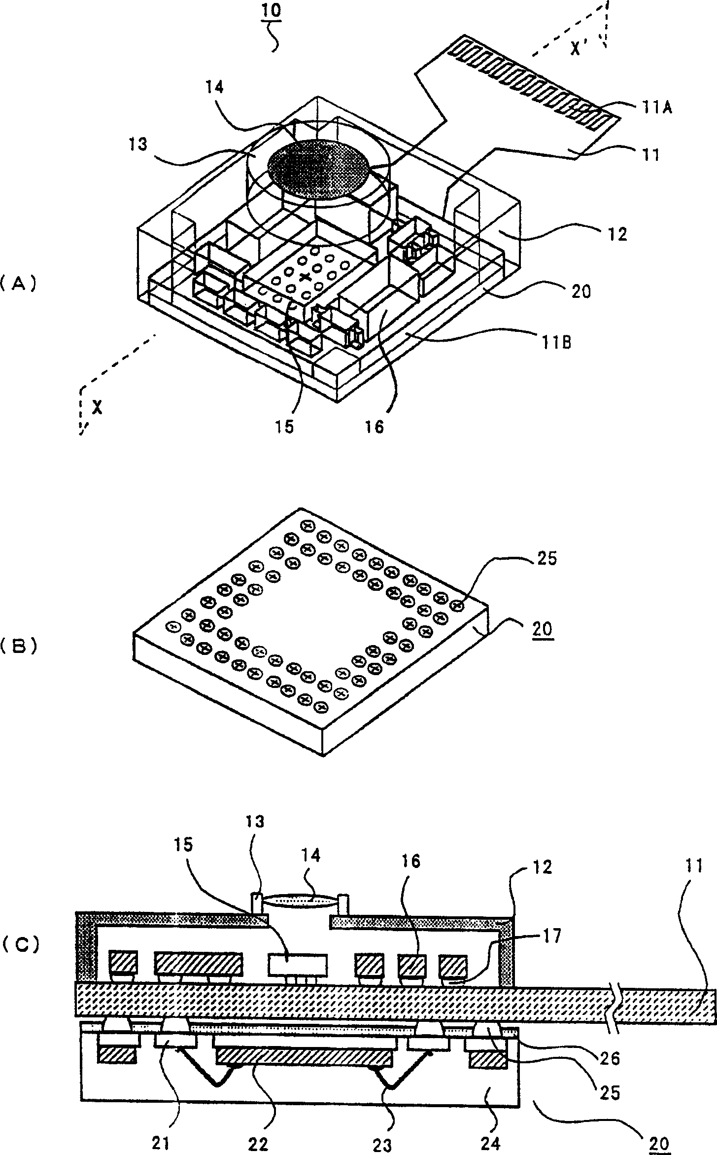
[0046] (A first embodiment for explaining the structure of the camera module 10)

[0047] refer to figure 1 The configuration and the like of the circuit device 10 of the present invention will be described. figure 1 (A) is a perspective view of the camera module 10, figure 1 (B) is a perspective view of the circuit device 10, figure 1 (C) is figure 1 (A) X-X' section view.

[0048] refer to figure 1A. The camera module 10 has the following structure. Namely comprising: the flexible board 11 of the resin sheet that has conductive circuit on both sides; The lens holder 12 that is arranged on the surface of flexible board 11; The circuit device 20 that is installed on the back side of flexible board 11; ; The lens 14 fixedly installed on the top of the lens holder 12, the circuit device 20 is equipped with a structure of semiconductor elements and passive elements electrically connected to the CCD. Such constituent elements will be described below.

[0049] refer t...


PUM


Abstract

CCD 15 and peripheral elements 16 are mounted on the surface of a mount portion 11B of a flexible sheet 11, and a circuit device 20 is mounted on the back surface of the mount portion 11B. DSP and a driver IC are installed in the circuit device 20, and the circuit device 20 is electrically connected to CCD 15 through electrical conductive paths 11E formed in the flexible sheet 11. CCD 15 and the peripheral elements 16 mounted on the mount portion 11B are covered by a lens mount 12. Accordingly, a camera module which is unified with the flexible sheet 11 is provided.

Description

technical field [0001] The present invention relates to a camera module and its manufacturing method, and relates to a thinned camera module obtained by integrating a resin sheet and a circuit device. Background technique [0002] In recent years, camera modules have been actively used in mobile phones, notebook computers, and the like. Therefore, the camera module is required to be smaller, thinner, and lighter. In the present invention, a camera module using a CCD as an image sensor will be described as an example. In addition, the same applies even if an imaging element other than a CCD (for example, a CMOS sensor, etc.) is used. [0003] refer to Figure 26 The configuration of a conventional camera module 100 will be described. First, the CCD 102 is mounted on the mounting substrate 101 . Then, above the CCD 102 , a lens 105 for collecting external light is fixed on a lens barrel 106 . In addition, the lens barrel 106 is held by a lens holder 107 mounted on the mou...

Claims


Application Information

Patent Timeline
IPC IPC(8): H05K1/02H01L23/12H04N5/225H05K1/18H05K3/46
CPCH01L24/97H04N5/2254H01L2924/15311H01L2924/19105H05K1/189H01L2224/48091H01L2224/48465H01L2224/49171H04N5/2253H01L2224/48227H01L2924/07802H01L2924/12042H01L2924/14H01L27/14618H01L27/14806H04N23/54H04N23/55H01L2924/00014H01L2924/00H04N23/00
Inventor 田村浩之小林健一
Owner SANYO ELECTRIC CO LTD
Features
  • R&D
  • Intellectual Property
  • Life Sciences
  • Materials
  • Tech Scout
  • Unparalleled Data Quality
  • Higher Quality Content
  • 60% Fewer Hallucinations
Learn More