

Active driving pixel structure and its checking method
A pixel structure and inspection method technology, applied in the direction of light source, electric light source, electroluminescent light source, etc., can solve problems such as difficult gap adjustment and light-emitting element defects
- Summary
- Abstract
- Description
- Claims
- Application Information
AI Technical Summary
Problems solved by technology
Method used
Image

Examples
Embodiment Construction
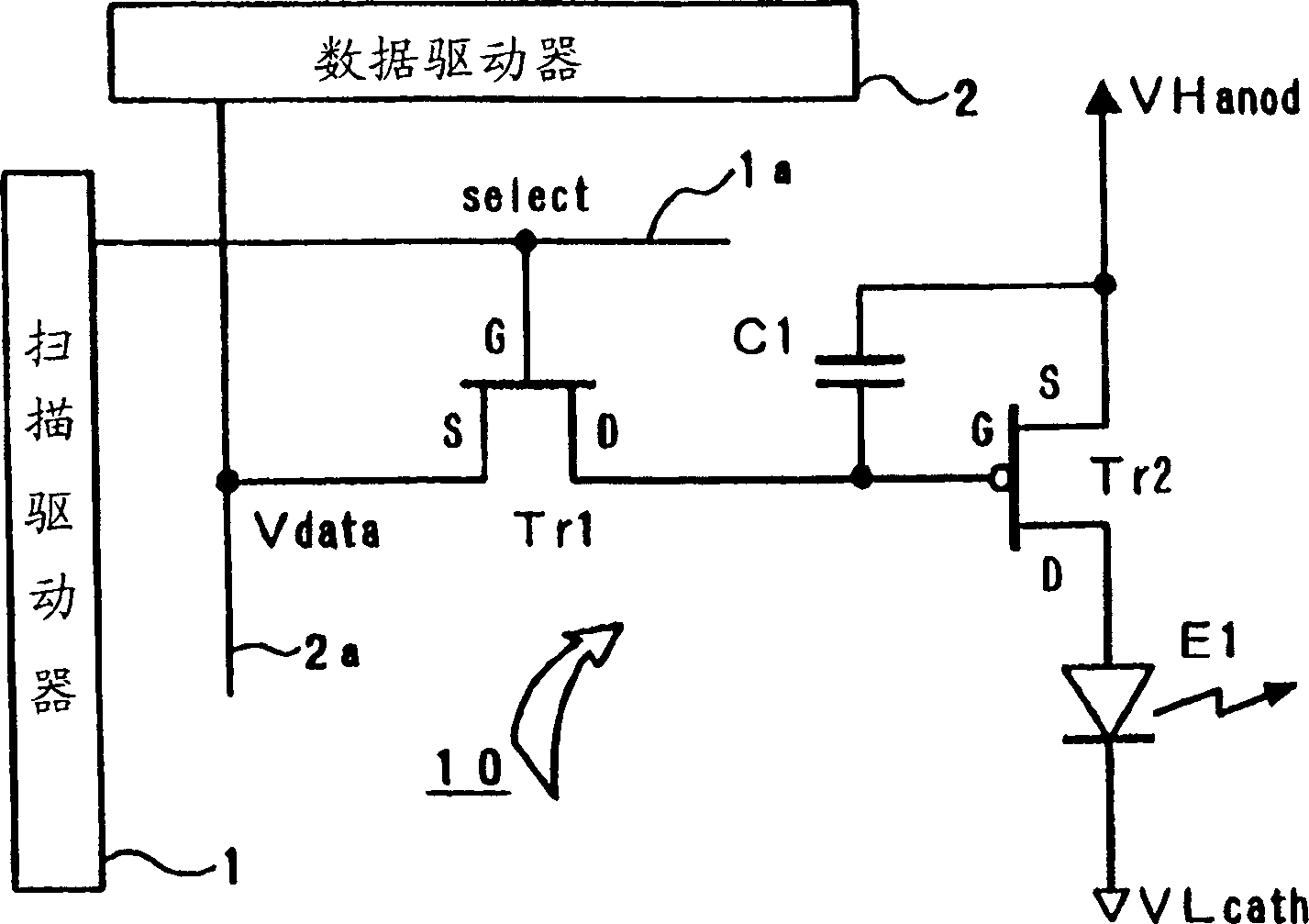
[0035] Hereinafter, the active driving pixel structure and inspection method of the present invention will be described according to the illustrated embodiment. In addition, in the following description, the same symbols are used to indicate the figure 1 The parts shown in 1 are equivalent to each other, so descriptions of various functions and operations are appropriately omitted.
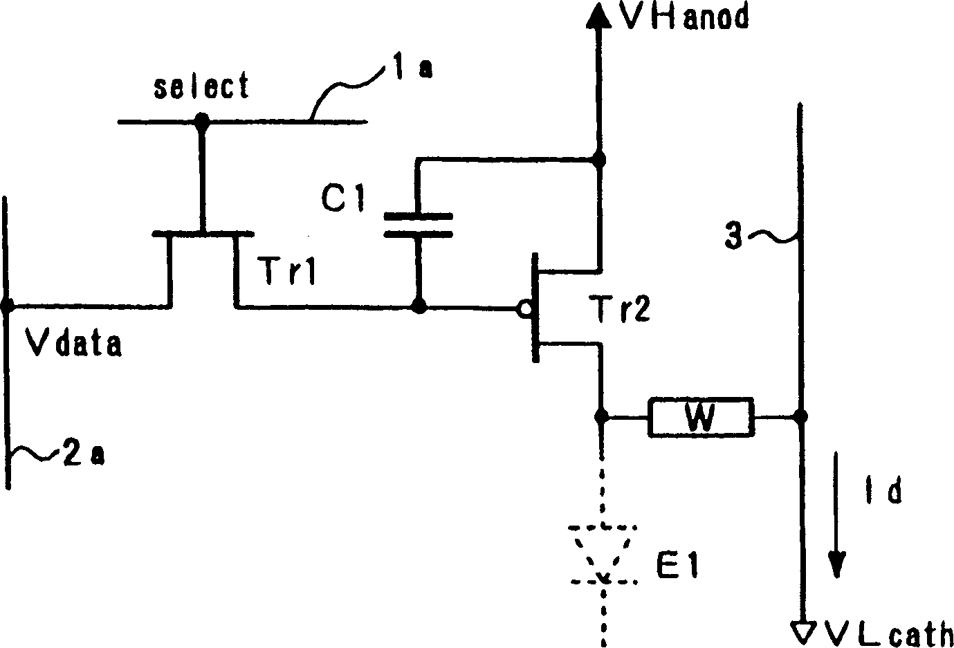
[0036] first, figure 2 It is a diagram showing the first embodiment of the active driving type pixel structure of the present invention. in the figure 2 The morphology shown shows the figure 1 The example shown is likewise referred to as a conductance-controlled circuit configuration. and, figure 2 The state shown shows the state of the semi-finished product before the film formation of the organic EL element E1.
[0037] exist figure 2 In the shown first embodiment, such a structure is formed that one end of the dummy load W for inspection is connected to the drain of the current outpu...
PUM
 Abstract
Description
Claims
Application Information