

Electro-optical device, method of driving electro-optical device, and electronic apparatus
一种电光学装置、驱动方法的技术,应用在辨认装置、电固体器件、彩色电视的零部件等方向,能够解决经时劣化、显示面板制造无序偏差等问题
- Summary
- Abstract
- Description
- Claims
- Application Information
AI Technical Summary
Problems solved by technology
Method used
Image

Examples
no. 1 approach
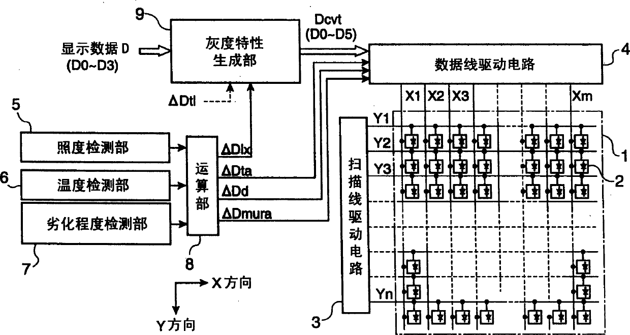
[0048] FIG. 1 is a block diagram of the structure of an electro-optical device according to this embodiment. For example, the display unit 1 is an active matrix type display panel in which electro-optical elements are driven by driving elements such as TFTs. In this display unit 1, pixels 2 of m dots×n lines are arranged in a matrix (two-dimensional plane). In addition, the display unit 1 is provided with scanning line groups Y1 to Yn each extending in the horizontal direction and data line groups X1 to Xm each extending in the vertical direction, and pixels 2 are arranged corresponding to their intersections. In this embodiment, although one pixel 2 is used as the minimum display unit of an image, one pixel 2 may be constituted by three sub-pixels of RGB like a color panel. In addition, in FIG. 1, a power supply line for supplying predetermined voltages Vdd and Vss to each pixel 2 and the like are omitted.
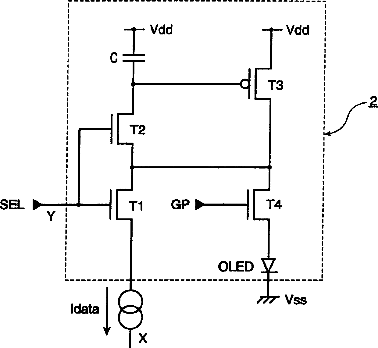
[0049] FIG. 2 is an example of a circuit diagram of the pixel 2. One pix...
no. 2 approach
[0097] FIG. 18 shows a configuration diagram of the current DAC 46 according to the second embodiment. The current DAC 46 includes a data signal generating unit 46a that generates a data signal to be supplied to the pixel 2 based on a current as a main body, and adding a correction value generating unit 46b and a drive voltage correcting unit 46d. The difference from the configuration example of FIG. 14 is that the structure of the data signal generation unit 46a is slightly different, and the drive voltage correction unit 46d is provided instead of the gradation correction unit 46c. Other than that, they are the same as the circuit elements of FIG. 14, so the same reference numerals are attached, and the description here is omitted.
[0098] The data signal generating unit 46a is provided between the data line X and the reference voltage Vss, and has a pair of switching transistors SW and driving transistors DR connected in series with the number of bits (that is, 6) of the conve...
no. 3 approach
[0104] Fig. 20 is an explanatory diagram of the outline features of the third embodiment. In this embodiment, the LUT process of the gradation characteristic generating unit 9 performs correction in consideration of two correction factors ΔDlx and ΔDtl, and the conversion data Dcvt is generated from the display data D. A part of the data signal generating section 46a constituting the pixel driving section does not consider the three correction factors ΔDd, ΔDmura, and ΔDta, and directly generates the data current Idata from the converted data Dcvt, and supplies it to the pixel 2 via the data line X.
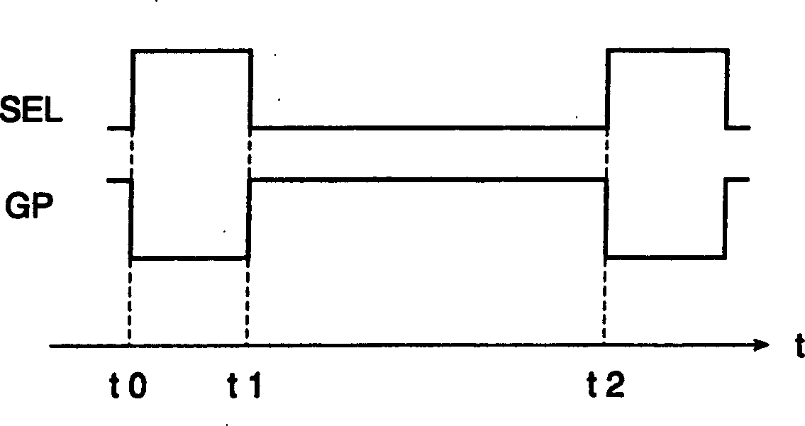
[0105] On the other hand, the driving period control section 10 constituting a part of the pixel driving section controls the driving period of the pixel 2 shown in FIG. 2 in consideration of three correction factors ΔDd, ΔDmura, and ΔDta. FIG. 21 is a driving timing chart of the pixel 2 as an example. Between the falling time t1 of the scanning signal SEL and the rising time of the ...
PUM
 Abstract
Description
Claims
Application Information