
Pland display having umbrella-shaped grid array structure and its manufacturing technology
A flat-panel display and array structure technology, which is applied in image/graphic display tubes, cold cathode manufacturing, electrode system manufacturing, etc., can solve the problems of high control gate voltage and large gate current, and achieve increased display brightness and reduced damage. , the effect of improving the success rate of production
- Summary
- Abstract
- Description
- Claims
- Application Information
AI Technical Summary
Problems solved by technology
Method used
Image

Examples
Embodiment Construction
[0033] The present invention will be further described below in conjunction with the accompanying drawings and embodiments, but the present invention is not limited to these embodiments.
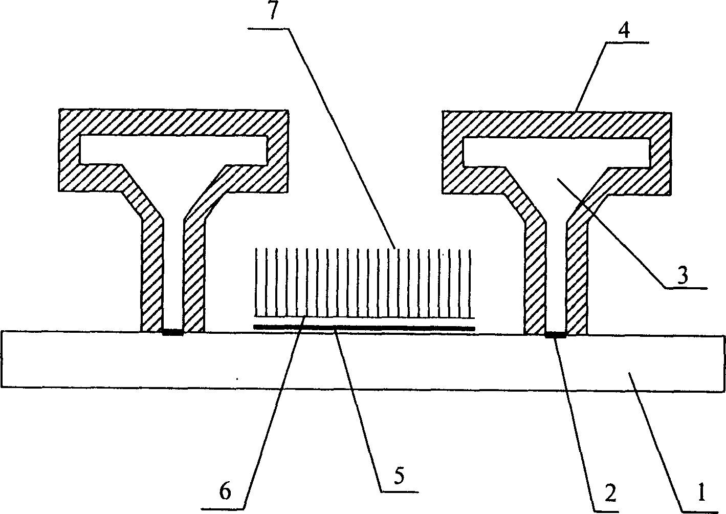
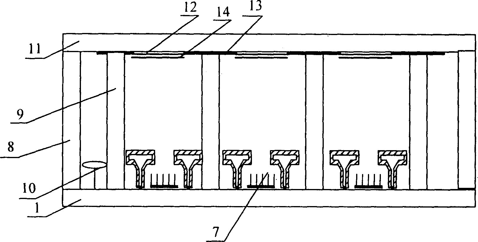
[0034] The present invention comprises a sealed vacuum chamber formed by a cathode panel 1, an anode panel 11 and surrounding glass enclosures 8; an anode conductive layer 12 photoetched on the anode panel 11 and a phosphor layer prepared on the anode conductive layer 12 14 . The support wall structure 9 and the accessory element 10 of the getter are fabricated on the cathode panel 1 with an umbrella-shaped grid array structure.
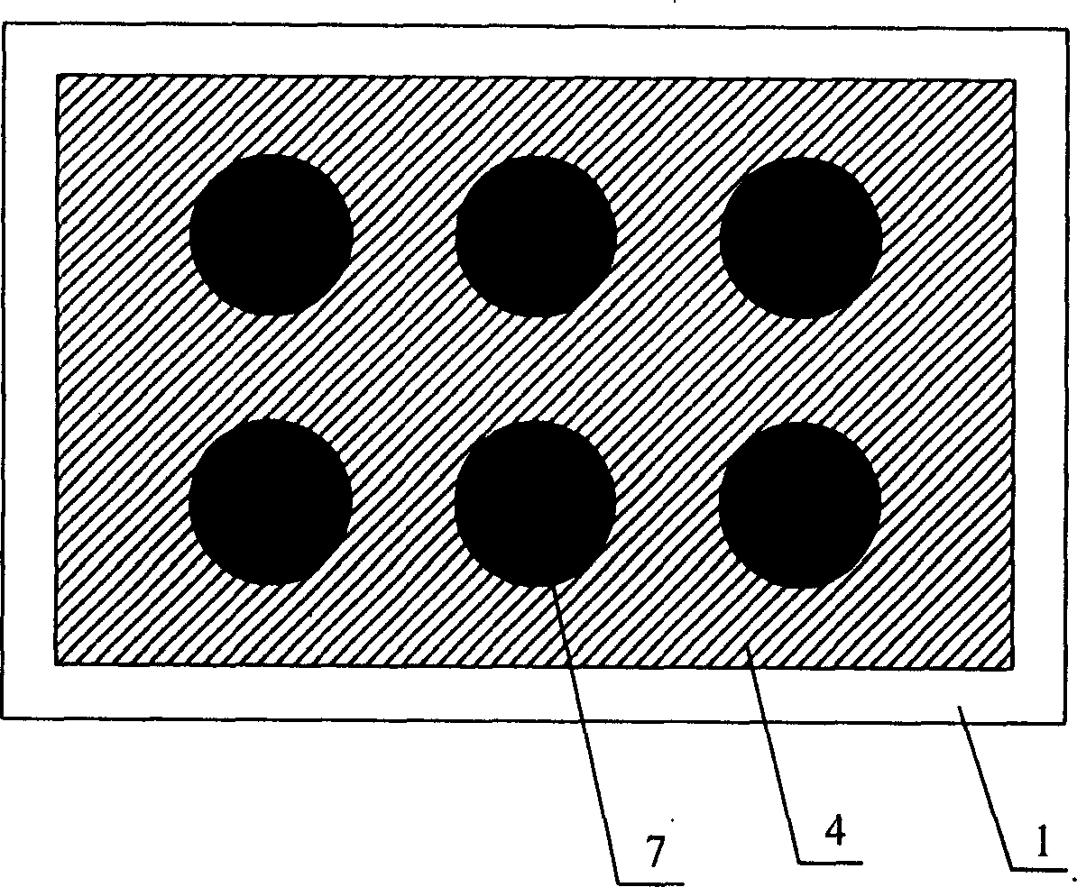
[0035] The umbrella gate structure includes a cathode panel 1, a gate conductive layer 2 arranged on the cathode panel 1, and a doped polysilicon layer 3 arranged on the gate conductive layer 2, wherein the shape of the doped polysilicon layer 3 is An umbrella structure, the insulating isolation layer 4 after etching covers all the doped polysilicon layer 3, the in...
PUM
 Abstract
Description
Claims
Application Information