Check patentability & draft patents in minutes with Patsnap Eureka AI!

Dummy pattern filling method

a filling method and pattern technology, applied in the field of ic fabrication, can solve the problems of layout seriously affecting the process and fabrication of the wafer, data ratio (dr) of the pattern, performance failure of components, or even functional failure, and achieve the effect of eliminating large-scale areas, and stable dr values of patterns

Active Publication Date: 2018-08-28
SHANGHAI HUAHONG GRACE SEMICON MFG CORP
View PDF24 Cites 0 Cited by
  • Summary
  • Abstract
  • Description
  • Claims
  • Application Information

AI Technical Summary

Benefits of technology

[0024]In this invention, at first, the rule of filling dummy patterns is determined based on the required DR value and isolation rules of patterns; then the Fields needed to fill dummy patterns are found out; then by changing the sizes, shapes and pitches of said dummy patterns in accordance with said filling rule, said Fields are filled (with dummy patterns). By means of changing dummy patterns, this invention is able to automatically match dummy patterns with Fields, thereby completing intelligent filling of dummy patterns. As a result, the DR value for all the filled dummy patterns after completing filling comes infinitely close to the required DR value, thus acquiring stable DR values of patterns and eliminating large-sized areas prohibiting filling of dummy patterns. In comparison with the Fixed Dummy Pattern Filling, the method of this invention is a Smart Dummy Pattern Filling.
[0025]Owing to the stableness of the DR values of patterns arising from this invention, the same etching process can be adopted for all the pattern configurations reaching the same required DR values of patterns. Therefore, good CD values can be achieved without any modifications of etching menus, thus not only eliminating process delays and enhancing efficiency, but also reducing difficulties in managing menus of etching processes and preventing losses arising from wrong uses of etching menus.
[0026]Since this invention can eliminate large-sized areas prohibiting filling of dummy patterns, said dishing effect after flattening by means of said CMP process can also be eliminated, thus avoiding process problems arising therefrom, such as such as the size reduction of their adjacent Actives, the deformation during the photoetching for the Gate at later stages, etc.

Problems solved by technology

With the development of semiconductor IC technologies and after reaching the very deep sub-micron level, the Data Ratio (DR) of the patterns on the mask, i.e., the layout seriously affects the process and fabrication of the wafer.
After the technological process is fixed, especially after the etching process is determined, the change of DR will directly affects the change of dimensions and appearance of etched lines, giving rise to the performance failure of components, or even the functional failure thereof.
It can be seen that after the parameters of the etching process are solidified, the change of DR will cause the value of CD to change, and will affect the component performance when the CD value deviates to a relatively large extent.
Therefore, some Fields cannot be filled with any dummy patterns.
However, it may not be able to close to the DR as required, or may not be able to overcome the CD deviation arising therefrom due to different layouts and different wiring for different products.
In this way, the delivery time of products may be directly affected, and it may also give rise to difficulties in managing numerous process menus.
Sometimes, it may even bring about huge losses as a result of wrong uses of menus.
This problem is particularly noticeable during etching.
After this area is flattened through a technological process of Chemical and Mechanical Polishing (CMP), a dishing effect will be resulted, bringing about a series of process problems, such as the size reduction of their adjacent Actives, the deformation during the photoetching for the Gate at later stages, etc.

Method used


Image

  • Dummy pattern filling method
  • Dummy pattern filling method

Examples


Embodiment Construction

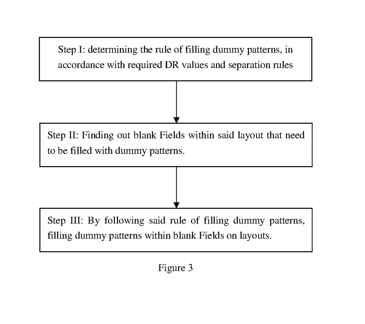
[0031]FIG. 3 is the flow diagram of the steps of filling dummy patterns for the Preferred Embodiment of this invention. The method of filling dummy patterns for the Preferred Embodiment of this invention includes the following steps:

[0032]Step I: Providing the required DR value and isolation rules for patterns of the layouts on respective layers; by following said required DR value and said isolation rules of patterns, determining the rule of filling dummy patterns, which ensures that the DR value of the patterns filled into the area in question satisfies said required DR value and said isolation rules of patterns by changing the sizes, shapes and pitches of said dummy patterns.

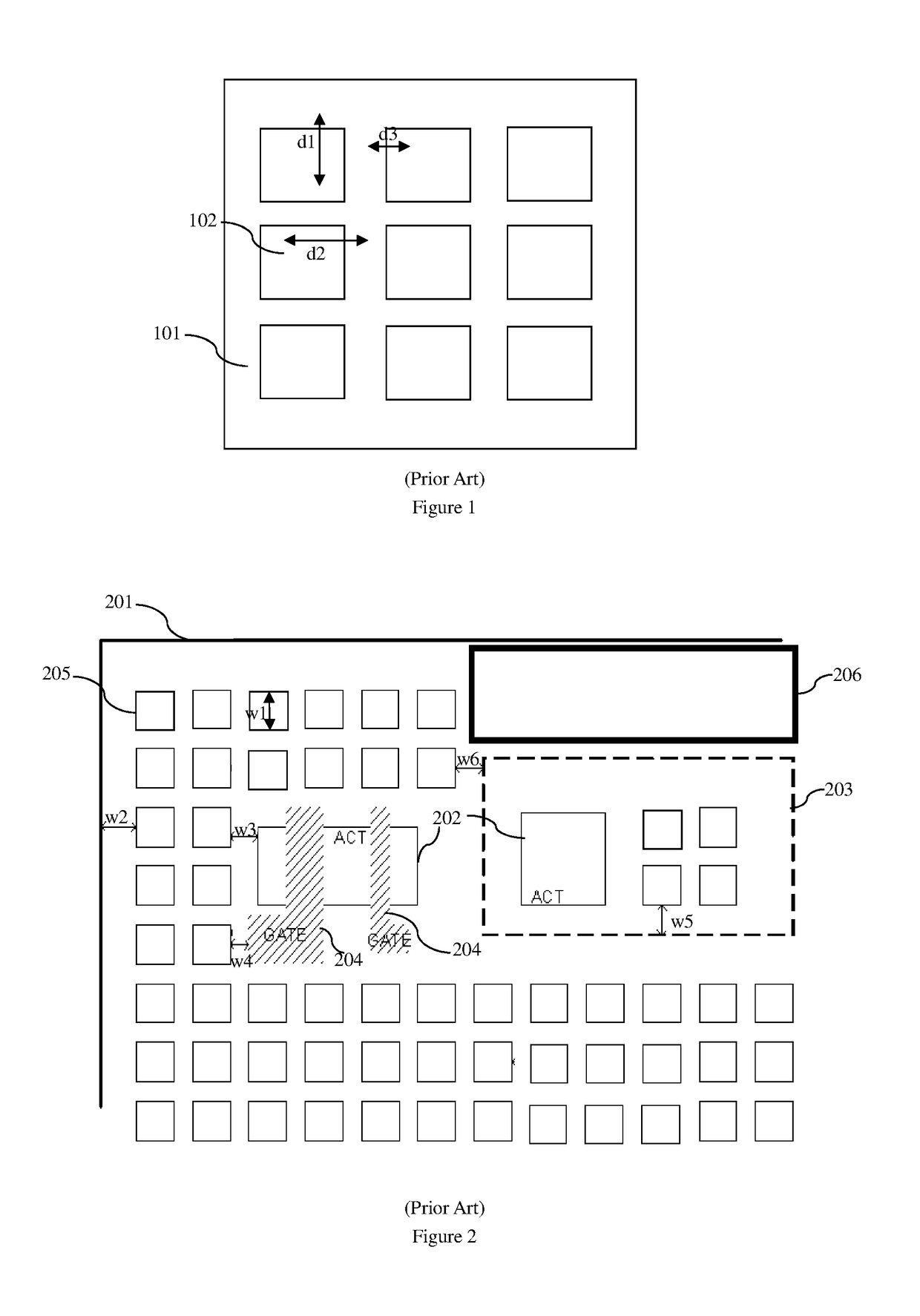
[0033]The layers with which said layouts correspond include the Active, the Gate and the Metals (layers).

[0034]Said required DR value of patterns is a fixed configuration.

[0035]Said isolation rule for patterns is determined by relevant design rules; said isolation rule for patterns includes the minimal pitch ...


PUM


Abstract

A dummy pattern filling method, including: Step I, determining the rule of filling dummy patterns, in accordance with required DR values and isolation rules of patterns; Step II, finding out blank Fields within said layout that need to be filled with dummy patterns; Step III, by following said rule of filling dummy patterns, filling dummy patterns within blank Fields on layouts. Implementing a Smart Dummy Pattern Filling, which enables the Data Ratio (DR) of dummy patterns to come infinitely close the required DR value after completing the filling of dummy patterns.

Description

CROSS REFERENCE TO RELATED APPLICATION[0001]The present application claims priority to Chinese Patent Application No. 201610373502.8 filed on May 31, 2016, the entirety of which is incorporated by reference herein.TECHNICAL FIELD[0002]This invention relates to a technological process of IC fabrication and is especially relates to a dummy pattern filling method.BACKGROUND OF INVENTION[0003]With the development of semiconductor IC technologies and after reaching the very deep sub-micron level, the Data Ratio (DR) of the patterns on the mask, i.e., the layout seriously affects the process and fabrication of the wafer. After the technological process is fixed, especially after the etching process is determined, the change of DR will directly affects the change of dimensions and appearance of etched lines, giving rise to the performance failure of components, or even the functional failure thereof. Practical examples in Table 1 show the huge deviations of the Critical Dimension (CD) of t...

Claims


Application Information

Patent Timeline
Patent Type & Authority Patents(United States)
IPC IPC(8): G06F17/50H01L27/02
CPCG06F17/5072H01L27/0207G06F17/5081G06F30/392G06F30/398
Inventor CHEN, HUALUNKONG, WEIRAN
Owner SHANGHAI HUAHONG GRACE SEMICON MFG CORP
Features
  • R&D
  • Intellectual Property
  • Life Sciences
  • Materials
  • Tech Scout
  • Unparalleled Data Quality
  • Higher Quality Content
  • 60% Fewer Hallucinations
Learn More