Face down dual sided chip scale memory package
- Summary
- Abstract
- Description
- Claims
- Application Information
AI Technical Summary
Benefits of technology
Problems solved by technology
Method used
Image

Examples
Embodiment Construction
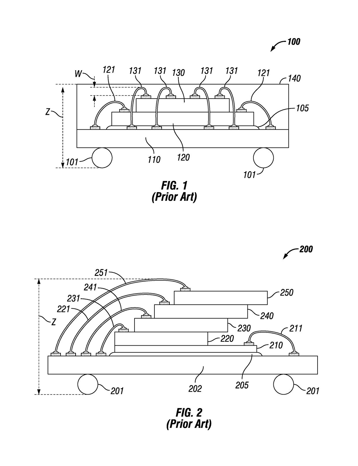
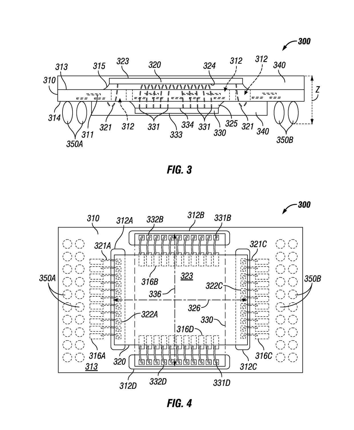
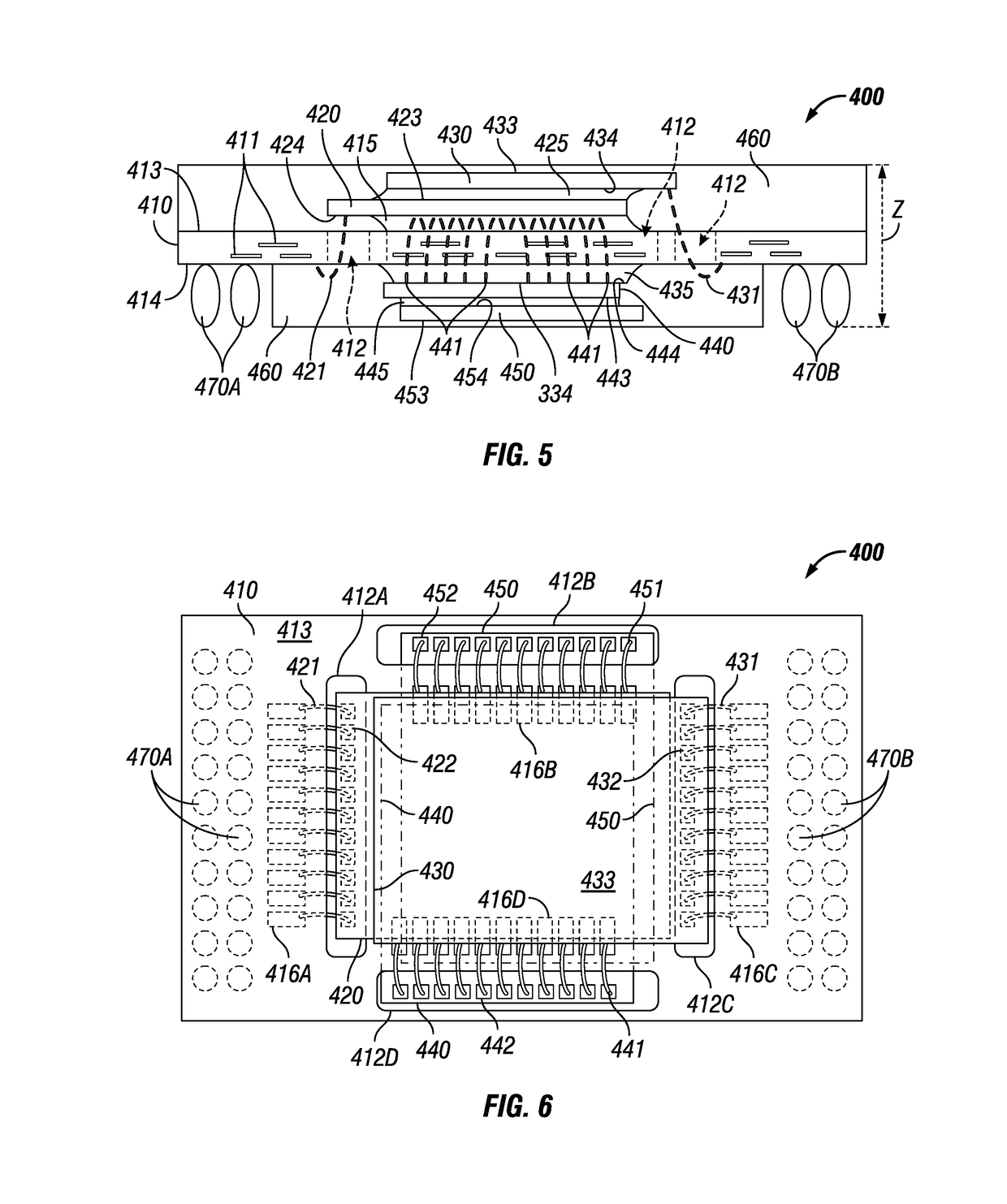
[0019]FIG. 3 shows a schematic of an embodiment of a semiconductor device 300 having an interposer 310 with a top side, or first side 313, and a bottom side, or second side 314. The interposer 310 includes internal connections 311 that may be used to distribute power, ground, and / or output / input signals within the interposer 310 and to the dies 320, 330 as would be appreciated by one of ordinary skill in the art. The device 300 includes a first semiconductor die 320, also referred to as first die 320, positioned above the first side 313 of the interposer 310 and a second semiconductor die 330, also referred to as second die 330, positioned below the second side 314 of the interposer 310. An adhesive layer 315 attaches the first die 320 to the first side 313 of the interposer 310 and an adhesive layer 325 attaches the second die 330 to the second side 314 of the interposer 310. The first and second dies 320, 330 are electrically connected to the interposer 310. The second side 314 of...
PUM
 Abstract
Description
Claims
Application Information
 - R&D Engineer
- R&D Manager
- IP Professional
- Industry Leading Data Capabilities
- Powerful AI technology
- Patent DNA Extraction
Browse by: Latest US Patents, China's latest patents, Technical Efficacy Thesaurus, Application Domain, Technology Topic.
© 2024 PatSnap. All rights reserved.Legal|Privacy policy|Modern Slavery Act Transparency Statement|Sitemap