Display panel and display device

a display panel and display device technology, applied in non-linear optics, instruments, optics, etc., can solve problems such as abnormal image display and lowering of the contrast of the entire display panel, and achieve the effect of reducing the size of the light transmission zone and reducing the problem of image display abnormality

Active Publication Date: 2019-07-09
TCL CHINA STAR OPTOELECTRONICS TECH CO LTD
View PDF12 Cites 0 Cited by
  • Summary
  • Abstract
  • Description
  • Claims
  • Application Information

AI Technical Summary

Benefits of technology

[0016]Compared to the prior art, this application provides a display panel, which possesses at least the following advantages:
[0017]The display panel is structured to reduce the size of the light transmission zone of the thin-film transistor layer or to increase the size of the light blocking zone of the color filter substrate in order to reduce issues of abnormality of image displaying caused by deviation of light from a corresponding color resist sub-pixel area, or even projection onto other color resist sub-pixel areas adjacent thereto, at the time when light transmits from the light transmission zone of the thin-film transistor layer to get incident onto the color filter substrate.

Problems solved by technology

Such a mechanism leads to lowering of contrast of the entire display panel so that it is necessary to place the polarization structure between the color filter layer and the liquid crystal layer.
This would result in majority of the incident light deviating from the area of the corresponding color sub-pixel and projecting toward other areas of adjacent sub-pixels, leading to cross-talking of light among the sub-pixel areas and causing abnormal displaying of images.

Method used


Image

  • Display panel and display device
  • Display panel and display device
  • Display panel and display device

Examples


first example embodiment

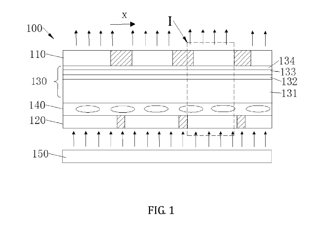
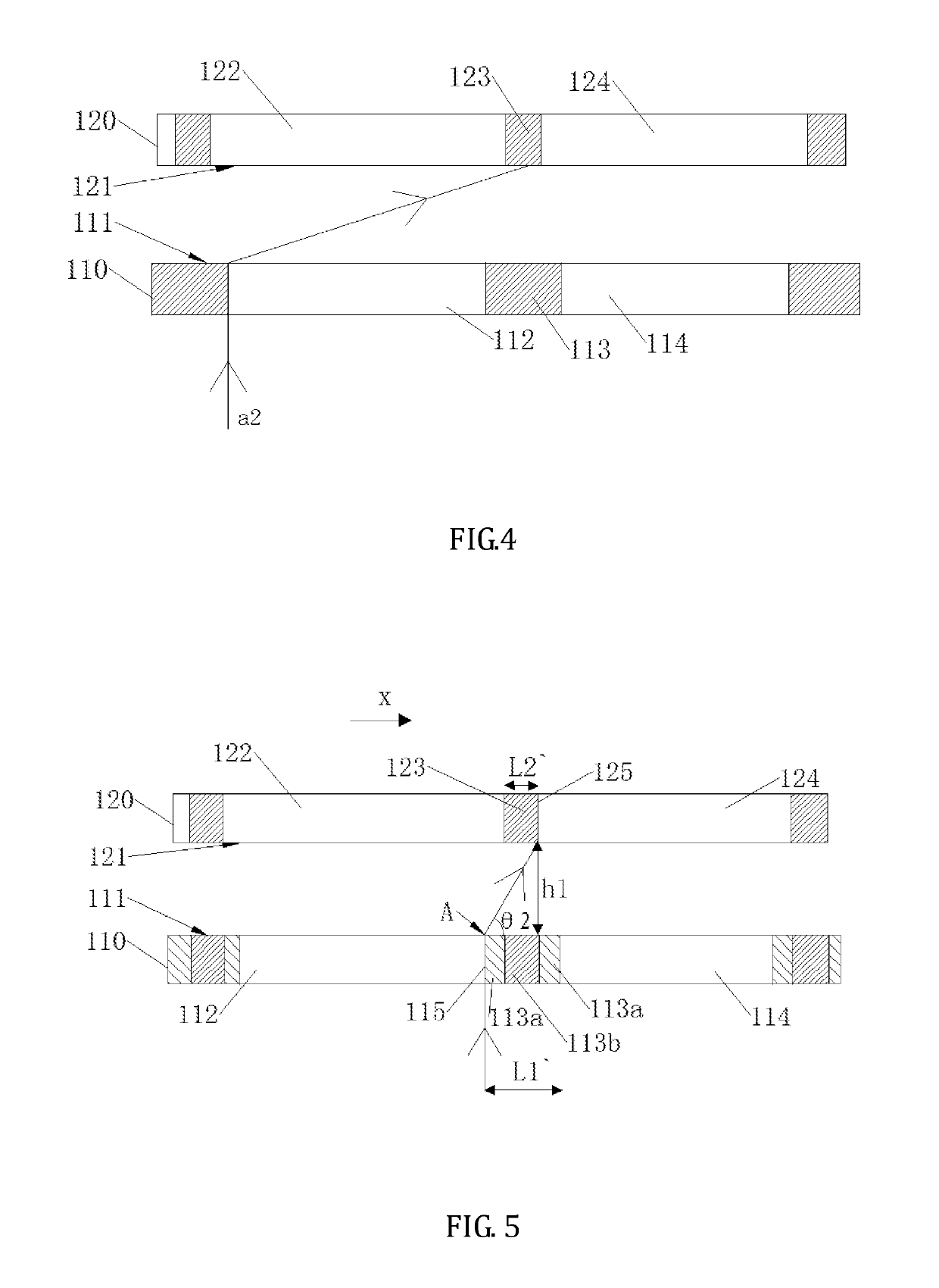
[0036]Referring to FIG. 5, the first substrate 110 is made a thin-film transistor layer, and the second substrate 120 is made a color filter substrate. The backlight source 150 is arranged on one side of the thin-film transistor layer 110 that is distant from the color filter substrate 120. The backlight source 150 emits first light a1 transmitting through the third light transmission zone 122 to project onto the first light transmission zone 112. The first light transmission zone 112 and the second light transmission zone 114 are opening areas in the thin-film transistor layer 110 and the first light blocking zone 113 is a metal wiring area (including a thin-film transistor and metal wiring corresponding thereto). The third light transmission zone 122 and the fourth light transmission zone 124 are color resist sub-pixel areas and the second light blocking zone 123 is a black matrix.

[0037]Generally, the light transmission zones of the thin-film transistor layer 110 and the light tra...

second example embodiment

[0043]Referring to FIG. 7, the first substrate 110 can alternatively be a color filter substrate and the second substrate 120 is a thin-film transistor layer. The display substrate may further comprises a backlight source 150, such that the backlight source 150 is arranged at one side of the thin-film transistor layer that is distant from the color filter substrate. The backlight source 150 emits second light a2 transmitting through the first light transmission zone 112 to project onto the third light transmission zone 122.

[0044]The first light transmission zone 112 and the second light transmission zone 114 can be color resist sub-pixel areas and the first light blocking zone 113 can be a black matrix. The third light transmission zone 122 and the fourth light transmission zone 124 can be opening areas in the thin-film transistor layer 120 and the second light blocking zone 123 is a second metal wiring zone, wherein a projection of the first light blocking zone 113 cast onto the se...


PUM

PropertyMeasurementUnit
angleaaaaaaaaaa
angleaaaaaaaaaa
incident angleaaaaaaaaaa

Abstract

A display panel includes a liquid crystal layer arranged between first and second substrates. The first substrate includes, consecutively connected, a first light transmission zone, a first light blocking zone, and a second light transmission zone. The second substrate includes, consecutively connected, a third light transmission zone, a second light blocking zone, and a fourth light transmission zone. A projection of the first light blocking zone cast on the second substrate has an area covering the second light blocking zone. The first light blocking zone functions to block, when first light is projected onto the first light transmission zone, the first light from projecting onto the second light transmission zone, and the second light blocking zone functions to block, when second light is projecting onto the third light transmission zone, the second light from projecting onto the fourth light transmission zone. A display device is also provided.

Description

CROSS REFERENCE TO RELATED APPLICATIONS[0001]This application claims the priority of Chinese Patent Application No. 2017106473676 filed on Aug. 1, 2017, titled “Display Panel and Display Device”, the disclosure of which is incorporated herein by reference in its entirety.BACKGROUND OF THE INVENTION1. Field of the Invention[0002]The present invention relates to the field of liquid crystal display technology, and more particularly to a display panel and a display device having the display panel.2. The Related Arts[0003]In a traditional display panel, upper and lower polarizers are often provided on two opposite sides of a color filter layer for forming, in combination with liquid crystal optics, a color luminous panel. In new technical development, it is necessary to place a polarization structure between the color filter layer and a liquid crystal layer. This is done for the consideration of two situations: (1) The color filter layer is generally made up of components including pigme...

Claims


Application Information

Patent Timeline
Patent Type & Authority Patents(United States)
IPC IPC(8): G02F1/1335G02F1/1362G02F1/135
CPCG02F1/133512G02F1/133514G02F1/136286G02F1/136209G02F2001/136218G02F2001/1351G02F1/1335G02F1/133516G02F1/1351G02F1/136218
Inventor CHEN, LIXUAN
Owner TCL CHINA STAR OPTOELECTRONICS TECH CO LTD
Why Eureka
Try Eureka