

Image processing method and device for LED display screen
- Summary
- Abstract
- Description
- Claims
- Application Information
AI Technical Summary
Benefits of technology
Problems solved by technology
Method used
Image

Examples
first embodiment
[0049]FIG. 5 is a flowchart of an image processing method for an LED display according to the disclosure. As shown in FIG. 5, the method includes the following steps.
[0050]Step S501: Original image data is received.
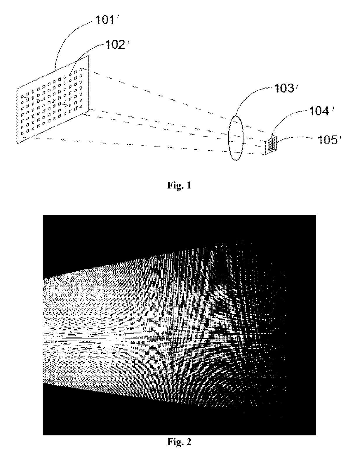
[0051]The original image data is a data of each frame of image of an image video resource, and is used for representing information of the image video resource such as color information and position information of the image video resource. Image effects such as the color, contour, position, luminance and definition of an image of the image video resource are determined by means of the original image data. The original image data may be acquired by digital photographic equipment. For example, the original image data may be acquired by means of digital photographic equipment, a camera and a photographic device of a mobile phone. The digital photographic equipment includes an optical lens, a photosensitive device for photoelectric conversion, photosensitive pixels particles ...
second embodiment
[0067]FIG. 13 is a flowchart of an image processing method for an LED display according to the disclosure. As shown in FIG. 13, the method includes the following steps.
[0068]Step S1301: Digital photographic equipment acquires image video resource.
[0069]Original image data may be acquired by the digital photographic equipment. For example, the original image data is acquired by a digital camera, a camera, a photographic device of a mobile phone, etc. Information of the original pixel is acquired according to the original image data.
[0070]Step S1302: A preset algorithm is determined.
[0071]The preset algorithm may execute computation on the color information of the original pixel and the position information of the original pixel to obtain the target pixel, such that the target pixel is a discrete LED pixel point which is distributed not in a preset rule, and meanwhile, the color information of the target pixels is adjusted. The original pixel is a pixel distributed on an LED display s...
PUM
 Abstract
Description
Claims
Application Information