Method for preparing ZnO thin films with buffer layers

A buffer layer and composite buffer layer technology, applied in chemical instruments and methods, from chemically reactive gases, single crystal growth, etc., can solve problems such as large mismatch of thermal expansion coefficients, and achieve improved crystallization quality, high repeatability, and The effect of simple process

Inactive Publication Date: 2018-09-21
(CNBM) BENGBU DESIGN & RES INST FOR GLASS IND CO LTD
View PDF0 Cites 2 Cited by
  • Summary
  • Abstract
  • Description
  • Claims
  • Application Information

AI Technical Summary

Problems solved by technology

However, due to the large mismatch between the lattice constant and thermal expansion coefficient of silicon wafers and ZnO, it is difficult to directly prepare high-performance ZnO thin films on silicon wafers to meet the requirements of electronic components.

Method used


Image

  • Method for preparing ZnO thin films with buffer layers

Examples


Embodiment Construction

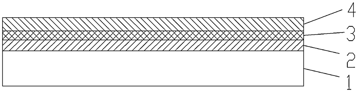
[0013] Such as figure 1 Shown, the invention provides a kind of preparation method with the ZnO thin film of buffer layer, comprises the following steps:

[0014] S1, cleaning the monocrystalline silicon substrate 1 to remove oil stains and impurities on the surface of the monocrystalline silicon substrate 1;

[0015] S2. Using magnetron sputtering equipment, using Al target as the target material, place the single crystal silicon substrate in the vacuum chamber of the magnetron sputtering equipment, and the vacuum degree reaches 3.0*10 -4 At Pa, the sputtering gas Ar is introduced for 5 minutes of pre-sputtering to make the Al target glow, so as to achieve the purpose of activating the target and removing the oxide on the target surface: after the pre-sputtering, the reaction gas N is introduced 2 , sputtering AlN buffer layer 2 on the surface of single crystal silicon substrate, sputtering power 100W, Ar flow rate 20sccm, N 2 The flow rate is 5sccm, the working pressure is...


PUM


Abstract

The invention discloses a method for preparing ZnO thin films with buffer layers. The method includes steps of S1, cleaning monocrystalline silicon substrates and removing oil stain and impurities onthe surfaces of the monocrystalline silicon substrates; S2, utilizing Al targets as target materials, placing the monocrystalline silicon substrates in vacuum chambers of magnetron sputtering equipment, filling the magnetron sputtering equipment with sputtering gas Ar and reaction gas N2, and sputtering coating AlN buffer layers on the surfaces of the monocrystalline silicon substrates; S3, utilizing Al targets and ZnO targets as target materials, and sputtering coating composite buffer layers comprising AlN and ZnO on the surfaces of the AlN buffer layers; S4, utilizing ZnO targets as targetmaterials, and sputtering coating ZnO film layers on the surfaces of the composite buffer layers to obtain the ZnO thin films with the buffer layers. The method has the advantages that the ZnO film layers can be prevented from being in direct contact with the monocrystalline silicon substrates, and accordingly the crystallization quality of the plated ZnO film layers can be improved; integral procedures are simple magnetron sputtering film coating, are simple and are high in controllability and repeatability.

Description

technical field [0001] The invention relates to a preparation method of a ZnO film with a buffer layer. Background technique [0002] ZnO is a self-activated wide bandgap semiconductor material with a room temperature gap of 3.37eV. It also has higher thermal stability and exciton binding energy, so its excellent photoelectric properties, pressure-sensitive and gas-sensitive properties make it have broad application prospects in many fields such as ultraviolet detectors and solar cells. [0003] Silicon wafer is the core material in current electronic components, and the price is very low, so the preparation of high-performance ZnO thin films on silicon wafers has an attractive prospect. However, due to the large mismatch between the lattice constant and the thermal expansion coefficient of silicon wafers and ZnO, it is difficult to directly prepare high-performance ZnO thin films on silicon wafers to meet the requirements of electronic components. Contents of the inventi...

Claims


Application Information

Patent Timeline
Patent Type & Authority Applications(China)
IPC IPC(8): C30B29/16C30B25/06C30B25/18
CPCC30B25/06C30B25/18C30B29/16
Inventor 沈洪雪姚婷婷杨勇李刚
Owner (CNBM) BENGBU DESIGN & RES INST FOR GLASS IND CO LTD
Why Eureka
Try Eureka