Switching regulator including an offset enabled comparison circuit

a technology of switching regulator and offset enabled comparison circuit, which is applied in the direction of electric variable regulation, process and machine control, instruments, etc., can solve the problems of ripple voltage increase and error voltage verr decrease, and achieve the effect of preventing unnecessary operation of the switching element during pfm operation and reducing ripple voltage in output voltag

Active Publication Date: 2019-09-17
ABLIC INC
View PDF29 Cites 2 Cited by
  • Summary
  • Abstract
  • Description
  • Claims
  • Application Information

AI Technical Summary

Benefits of technology

[0030]According to the switching regulator of the present invention, an offset is provided to the input of the PFM comparison circuit for a given period so that the effect of compensation for a response delay of the PFM comparison circuit is obtained, preventing unnecessary operation of the switching element during PFM operation. A ripple voltage in the output voltage can accordingly be reduced.

Problems solved by technology

The turning on of the PMOS transistor 530 causes the output voltage VOUT to exceed the prescribed voltage value in a short time because the load current at this point is small, with the result that the error voltage VERR decreases.
However, the sharp rise of the output voltage VOUT widens the extent of the rise of the output voltage VOUT that is caused by executing the switching operation of the PMOS transistor 530 once, with the result that the ripple voltage increases.

Method used


Image

  • Switching regulator including an offset enabled comparison circuit
  • Switching regulator including an offset enabled comparison circuit
  • Switching regulator including an offset enabled comparison circuit

Examples


first embodiment

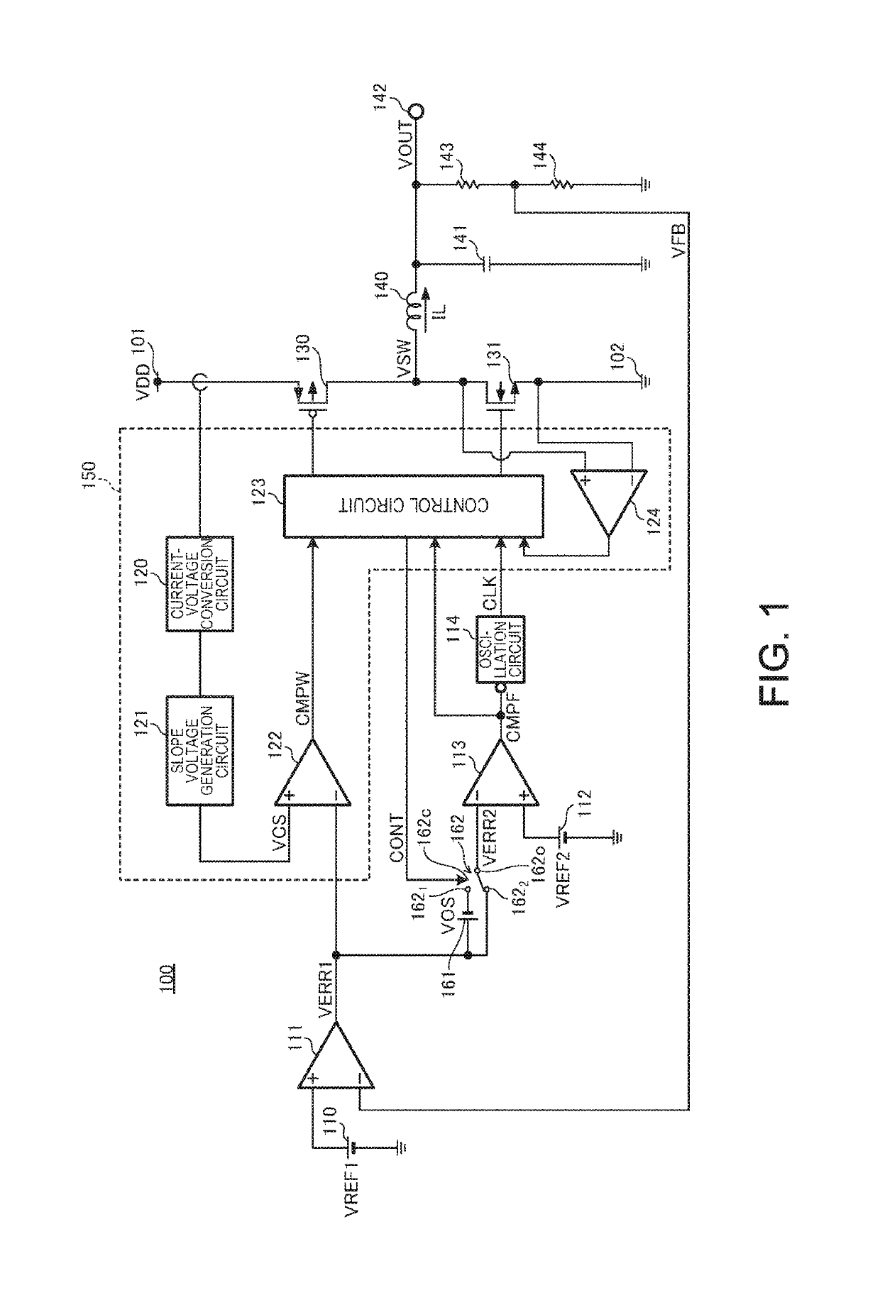
[0038]FIG. 1 is a circuit diagram for illustrating a switching regulator 100 according to the present invention.

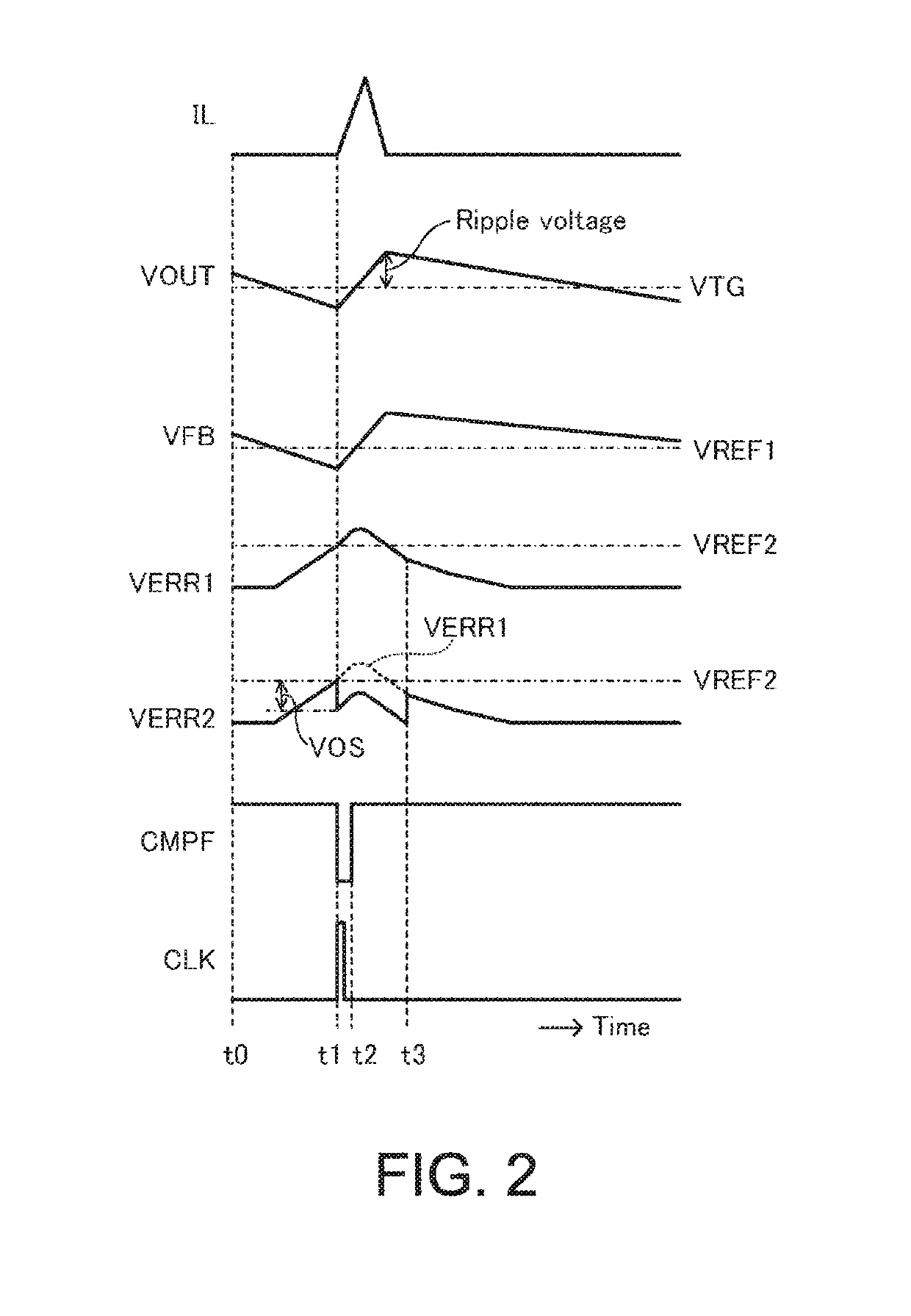
[0039]The switching regulator 100 according to the first embodiment includes a power supply terminal 101, a ground terminal 102, a reference voltage source 110, an error amplification circuit 111, a reference voltage source 112, a PFM comparison circuit 113, an oscillation circuit 114, a PMOS transistor 130 (also referred to as “switching element”), an NMOS transistor 131 (also referred to as “synchronous rectification element”), an inductor 140, a capacitor 141, resistors 143 and 144, an output terminal 142, a PWM conversion circuit 150 which includes a current-voltage conversion circuit 120, a slope voltage generation circuit 121, a PWM comparison circuit 122, a control circuit 123, and a reverse flow detection circuit 124, an offset voltage source 161 which is a constant voltage source, and a switch 162 which includes a terminal 162o, a first terminal 1621, a second ter...

second embodiment

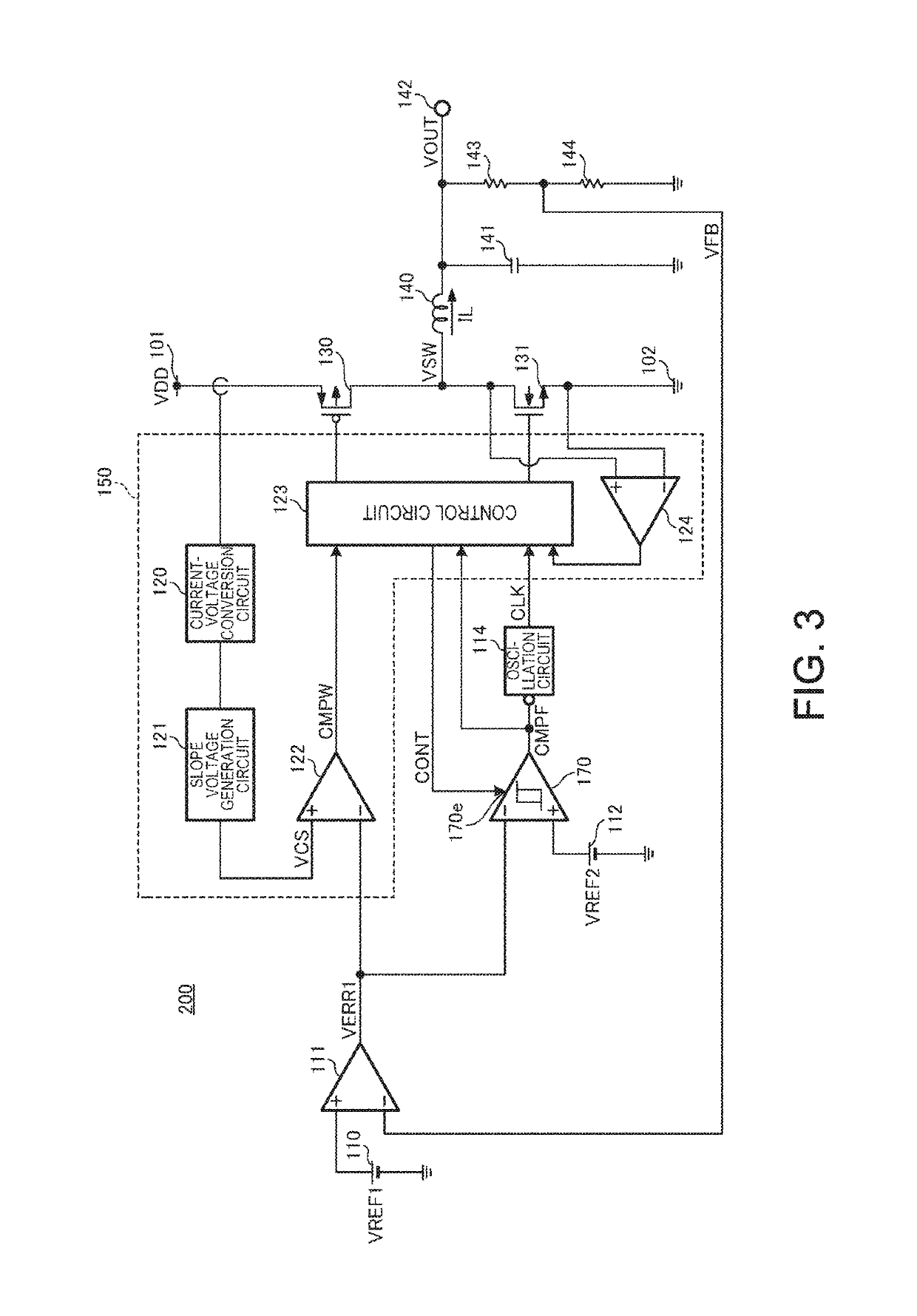
[0065]A switching regulator 200 according to the present invention is described next with reference to FIG. 3.

[0066]The switching regulator 200 according to the second embodiment is configured by removing the offset voltage source 161 and the switch 162 from the switching regulator 100 according to the first embodiment and replacing the PFM comparison circuit 113 with a PFM comparison circuit 170 with hysteresis.

[0067]The rest of the configuration of the switching regulator 200 is the same as that of the switching regulator 100 of FIG. 1, and the same components are therefore denoted by the same reference symbols to omit duplicate descriptions as appropriate.

[0068]In the PFM comparison circuit 170, an inverting input terminal is connected to the output of the error amplification circuit 111 and the inverting input terminal of the PWM comparison circuit 122, a non-inverting input terminal is connected to one end of the reference voltage source 112, an output is connected to the input...


PUM


Abstract

A switching regulator includes: an error amplification circuit configured to amplify a difference between a voltage based on the output voltage and a first reference voltage to output an error voltage; a PFM comparison circuit configured to compare the error voltage with a second reference voltage to output a comparison result signal at a first level or a second level, an offset being given to the error voltage for a given period in response to a change of the comparison result signal from the second level to the first level; an oscillation circuit configured to output a clock signal of a given frequency according to the first level of the comparison result signal, and to stop outputting the clock signal according to the second level of the comparison result signal; and a PWM conversion circuit configured to turn the switching element on at a prescribed pulse width.

Description

RELATED APPLICATIONS[0001]This application claims priority under 35 U.S.C. § 119 to Japanese Patent Application No. 2017-137918 filed on Jul. 14, 2017, the entire content of which is hereby incorporated by reference.BACKGROUND OF THE INVENTION1. Field of the Invention[0002]The present invention relates to a switching regulator.2. Description of the Related Art[0003]A circuit diagram of a switching regulator 500 of the related art is illustrated in FIG. 5.[0004]The switching regulator 500 of the related art includes a power supply terminal 501, a ground terminal 502, a reference voltage source 510, an error amplification circuit 511, a reference voltage source 512, a PFM comparison circuit 513, an oscillation circuit 514, a PMOS transistor 530, an NMOS transistor 531, an inductor 540, a capacitor 541, resistors 543 and 544, an output terminal 542, and a PWM conversion circuit 550 which includes a current-voltage conversion circuit 520, a slope voltage generation circuit 521, a PWM co...

Claims


Application Information

Patent Timeline
Patent Type & Authority Patents(United States)
IPC IPC(8): H02M1/00H02M3/158G05F1/595H02M3/156H02M1/36G05F1/10G05F1/46
CPCH02M3/156H02M2001/0041G05F1/10G05F1/595H02M2001/0025H02M1/36G05F1/46H02M3/158H02M2001/0032H02M1/14Y02B70/10H02M1/0041H02M1/0025H02M1/0032
Inventor TAKADA, KOSUKE
Owner ABLIC INC
Why Eureka
Try Eureka