

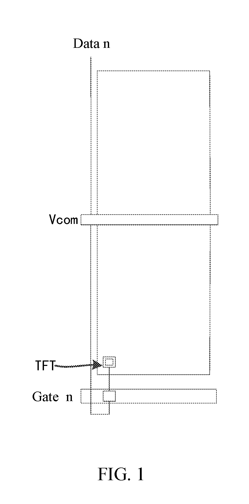
Pixel structure and display panel
a pixel and display panel technology, applied in the field of display techniques, can solve the problems of abnormal colors displayed, insufficient voltage of the pixel electrode, and the possibility of parasitic capacitors being generated, and achieve the effect of relieving the crosstalk
- Summary
- Abstract
- Description
- Claims
- Application Information
AI Technical Summary
Benefits of technology
Problems solved by technology
Method used
Image


Examples
example 1
[0069]the first conductive layer 11 and the second conductive layer 12 are formed of the conductive metals individually, and the third conductive layer 13 is formed of a conductive material. As another particular structure disposing the first conductive layer 11, the second conductive layer 12 and the third conductive layer 13 of the present application, the first conductive layer 11 and the second conductive layer 12 are both formed of the conductive metal of which the conductive metal has good conductive effect; the third conductive layer 13 formed of the transparent conductive material may also achieve a conductive effect. Further, the transparent conductive material of the present application may be formed of transparent conductive materials such as ITO, transparent conductive gel, which have good transmittance.
example 2
[0070]the first conductive layer 11 is formed of a conductive metal, and the second conductive layer 12 and the third conductive layer 13 are formed of a transparent conductive material individually. As yet another particular structure disposing the first conductive layer 11, the second conductive layer 12 and the third conductive layer 13 of the present application, the first conductive layer 11 is formed of a conductive metal of which the conductive metal has good conductive effect; the second conductive layer 12 and the third conductive layer 13 formed of the transparent conductive material may also achieve a conductive effect. Further, the transparent conductive material of the present application may be formed of transparent conductive materials such as ITO, transparent conductive gel, which have good transmittance.
example 3
[0071]the first conductive layer 11, the second conductive layer 12 and the third conductive layer 13 are formed of a transparent material individually. As yet another particular structure disposing the first conductive layer 11, the second conductive layer 12 and the third conductive layer 13 of the present application, all of the first conductive layer 11, the second conductive layer 12 and the third conductive layer 13 formed of the transparent conductive material may also achieve a conductive effect. Further, the transparent conductive material of the present application may be formed of transparent conductive materials such as ITO, transparent conductive gel, which have good transmittance.
[0072]In an embodiment of the present application, as shown in FIGS. 9-12, the second voltage line Vdc and the common line Vcom are partially overlapped spatially. In particular, the second voltage line is disposed to be overlapped with the common line in a region covered by the first conducti...
PUM
| Property | Measurement | Unit |
|---|---|---|
| voltage | aaaaa | aaaaa |
| voltage | aaaaa | aaaaa |
| voltage | aaaaa | aaaaa |
Abstract
Description
Claims
Application Information