Ultrasonic-wave probe, ultrasonic-wave diagnosis apparatus, and test method of ultrasonic-wave probe

a technology of ultrasonic probe and ultrasonic wave, which is applied in the field of operation method of reception/transmission separation switch, can solve problems such as increasing the number of cables

Active Publication Date: 2020-03-24
FUJIFILM HEALTHCARE CORP
View PDF10 Cites 0 Cited by
  • Summary
  • Abstract
  • Description
  • Claims
  • Application Information

AI Technical Summary

Benefits of technology

[0029]The internal-signal loopback test method in which the signal is attenuated and output while ensuring the withstand voltage in the transmission / reception separation switch so that the subsequent low-voltage reception circuit is not destroyed can be realized.
[0030]The problems, configurations, and effects other than those described above will be clarified from the description of the embodiments below.

Problems solved by technology

In this case, since it is practically impossible to increase the number of cables connecting the ultrasonic-wave probe and a main-device body to the second power, reception signals which have undergone reduction by phase-adjustment addition in the ultrasonic-wave probe have to be transferred to the main-body device via the cables.

Method used


Image

  • Ultrasonic-wave probe, ultrasonic-wave diagnosis apparatus, and test method of ultrasonic-wave probe
  • Ultrasonic-wave probe, ultrasonic-wave diagnosis apparatus, and test method of ultrasonic-wave probe
  • Ultrasonic-wave probe, ultrasonic-wave diagnosis apparatus, and test method of ultrasonic-wave probe

Examples


first embodiment

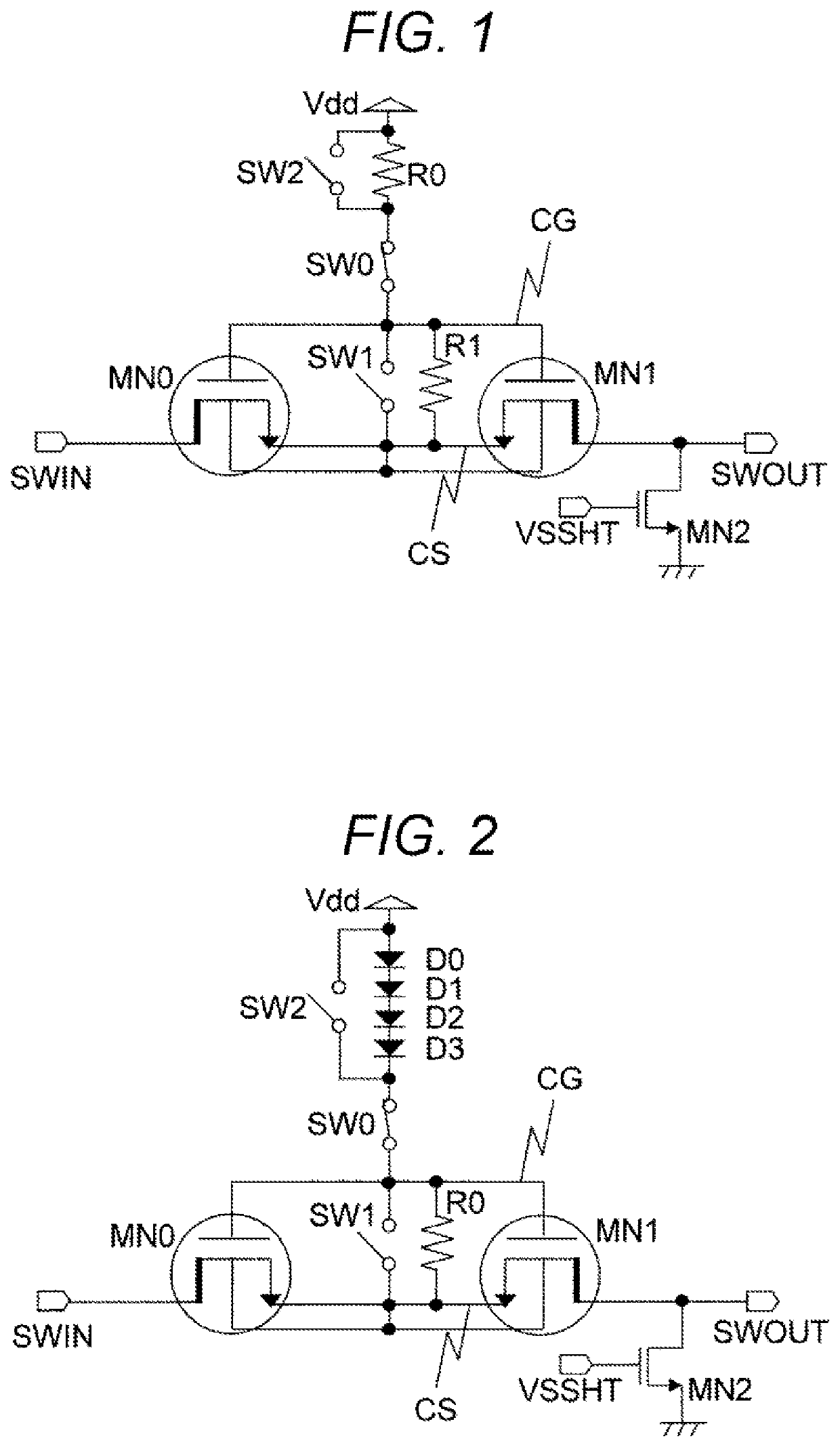
[0061]FIG. 2 shows an embodiment of the transmission / reception separation switch according to the present invention. In the configuration of FIG. 1, Vgs of MN0 and MN1 is generated by resistance voltage division by the resistance voltage division of R0 and R1. Since current flows from Vdd to R0 and R1 at this time, for example, in order to suppress the power consumption to the order of μW, it is necessary to set R0 and R1 to high resistances of the order of MΩ; and, although it depends on the sheet resistance of the resistance type prepared in a semiconductor process used, there is a concern that the area of the resistance increases.

[0062]Therefore, in the first, embodiment shown in FIG. 2, forward diodes D0, D1, D2, and D3 are used instead of R0 in FIG. 1. The internal-signal loopback test mode is obtained by turning SW0 on, SW1 off, and SW2 off, the forward voltage of the diodes at this point is Vf, and the potential of the common gate CG becomes (Mathematical Expression 3).

VCG=Vd...

second embodiment

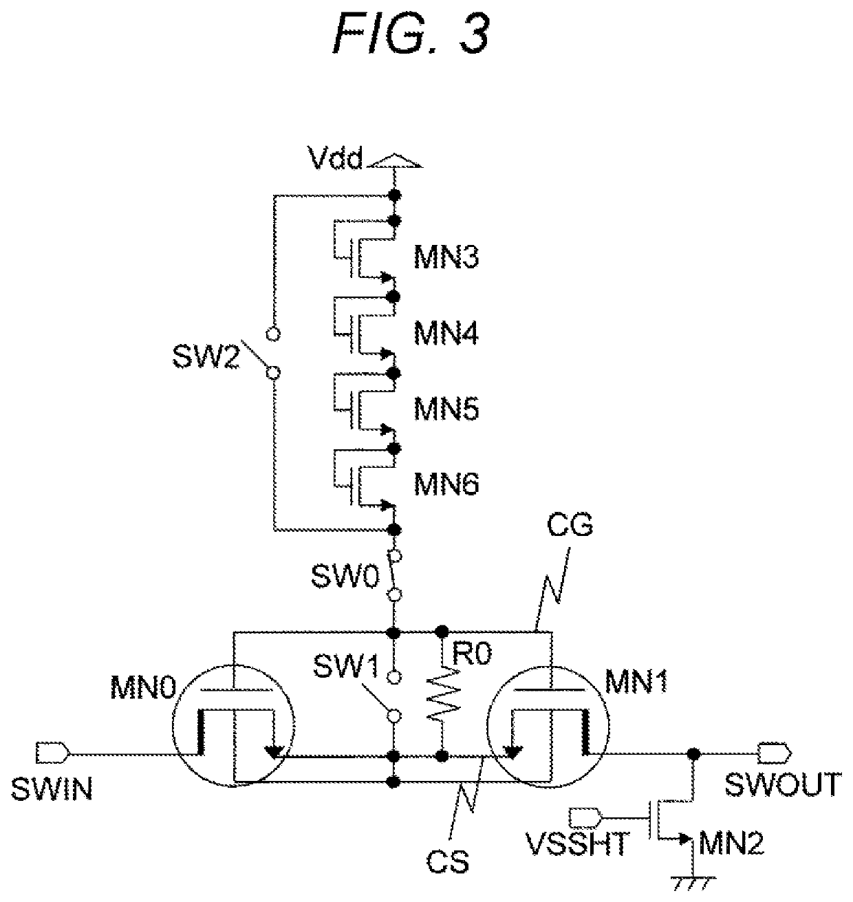
[0064]FIG. 3 shows an embodiment of the transmission / reception separation switch according to the present invention. In the first embodiment of FIG. 2, the forward diodes are used to lower the potential VCG of the common gate CG from Vdd. However, depending on the semiconductor process, diodes usable in the forward direction are designed on the assumption that a large current for rectification is to flow therethrough, and the area thereof may be large.

[0065]Therefore, in the second embodiment shown in FIG. 3, diode-connected MGSs in each of which a drain and a gate are connected to each other are used instead of the diodes of the first embodiment. The internal-signal loopback test mode is obtained by turning SW0 on, SW1 off, and SW2 off, gate-source voltages of MN3, MN4, MR5, and MN6 at this point are Vgsd, and the potential of the common gate CG becomes (Mathematical Expression 4).

VCG=Vdd−4·Vgsd  [Mathematical Expression 4]

[0066]VCG falls from Vdd by Vgsd of the diode-connected MOS...

third embodiment

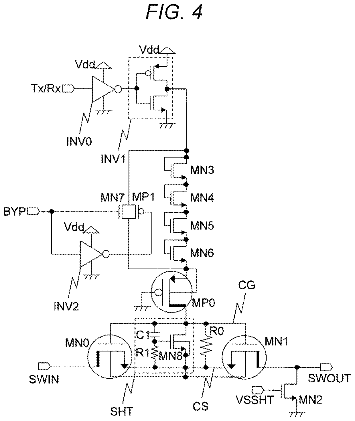
[0067]FIG. 4 shows a different embodiment of the transmission / reception separation switch according to the present invention. In this embodiment, the elements expressed as ideal switches in FIGS. 1, 2, and 3 are realized by actual MOSs. SW0 in FIG. 3 is replaced by MP0 in FIG. 4, SW1 in FIG. 3 is replaced by SHT in FIG. 4, and SW2 in FIG. 3 is replaced by MN7 and MP1 in FIG. 4.

[0068]In a case of transmission, the transmission circuit outputs high-voltage pulses of positive voltages or negative voltages; wherein, in a case in which a negative voltage is output, SWIN becomes a negative voltage, the drain in the structure of MN0 electrically serves as a source, and MN0 is turned on to be low to lower CS to a negative voltage. Therefore, CS and CG swing between the negative voltage and 0 V in the case of transmission. Therefore, a PMOS with a high withstand voltage has to be used as MP0 for switching the operations of transmission and reception. Also, the circuit connected to the source...


PUM


Abstract

A test for screening defects of a transmission / reception circuit in an IC is enabled at low cost, without withstand voltage violation, and without carrying out electrical contacts with many terminals connected to oscillators. In a transmission / reception separation switch circuit using transistors as switch elements, a potential of a gate is lowered in a test more than the potential in a case of reception to avoid gate-source withstand-voltage violation when a large-amplitude signal is input, and an internal-signal loopback test is carried out without destroying a reception circuit.

Description

TECHNICAL FIELD[0001]The present invention relates to an operation method of a reception / transmission separation switch for separating and protecting a reception circuit, which is formed by a low-voltage device, from a high-voltage signal output from a transmission circuit, which is formed by a high-withstand-voltage device, the switch mounted on an ultrasonic-wave probe, which is a constituent element of an ultrasonic-wave diagnosis apparatus. The present invention particularly relates to the techniques to realize a test method to test the transmission circuit and the reception circuit for each oscillator by using a signal subjected to loopback from the transmission circuit to the reception circuit in the ultrasonic-wave probe.BACKGROUND ART[0002]An ultrasonic-wave diagnosis apparatus is a non-invasive and highly safe medical diagnostic device for the human body and has a small apparatus scale compared with other medical image diagnosis apparatuses such as an X-ray diagnosis appara...

Claims


Application Information

Patent Timeline
Patent Type & Authority Patents(United States)
IPC IPC(8): H04B17/15H04B17/29A61B8/00
CPCH04B17/29A61B8/58A61B8/4494A61B8/4444H04B17/15G01R31/31716
Inventor KAJIYAMA, SHINYAIGARASHI, YUTAKAKATSUBE, YUSAKUNISHIMOTO, TAKUMA
Owner FUJIFILM HEALTHCARE CORP
Why Eureka
Try Eureka