Detecting printed circuit board design violations

a technology of printed circuit boards and design violations, applied in the field of printed circuit boards, can solve the problems of costly and/or inefficient design changes after a prototype is built and tested, and the design flaws are typically discovered, and the cost of time, material, labor and/or other resources, can be high and/or inconvenient to detect design flaws, and achieve the effect of detecting design flaws and detecting design flaws

Active Publication Date: 2020-01-14
IBM CORP
View PDF13 Cites 0 Cited by
  • Summary
  • Abstract
  • Description
  • Claims
  • Application Information

AI Technical Summary

Problems solved by technology

That is, design flaws are typically discovered after a prototype is built and tested.
Discovering / determining design flaws and making design changes after a prototype is built and tested can be costly and / or inefficient in terms of time, material, labor, and / or other resources.

Method used


Image

  • Detecting printed circuit board design violations
  • Detecting printed circuit board design violations
  • Detecting printed circuit board design violations

Examples


example 1

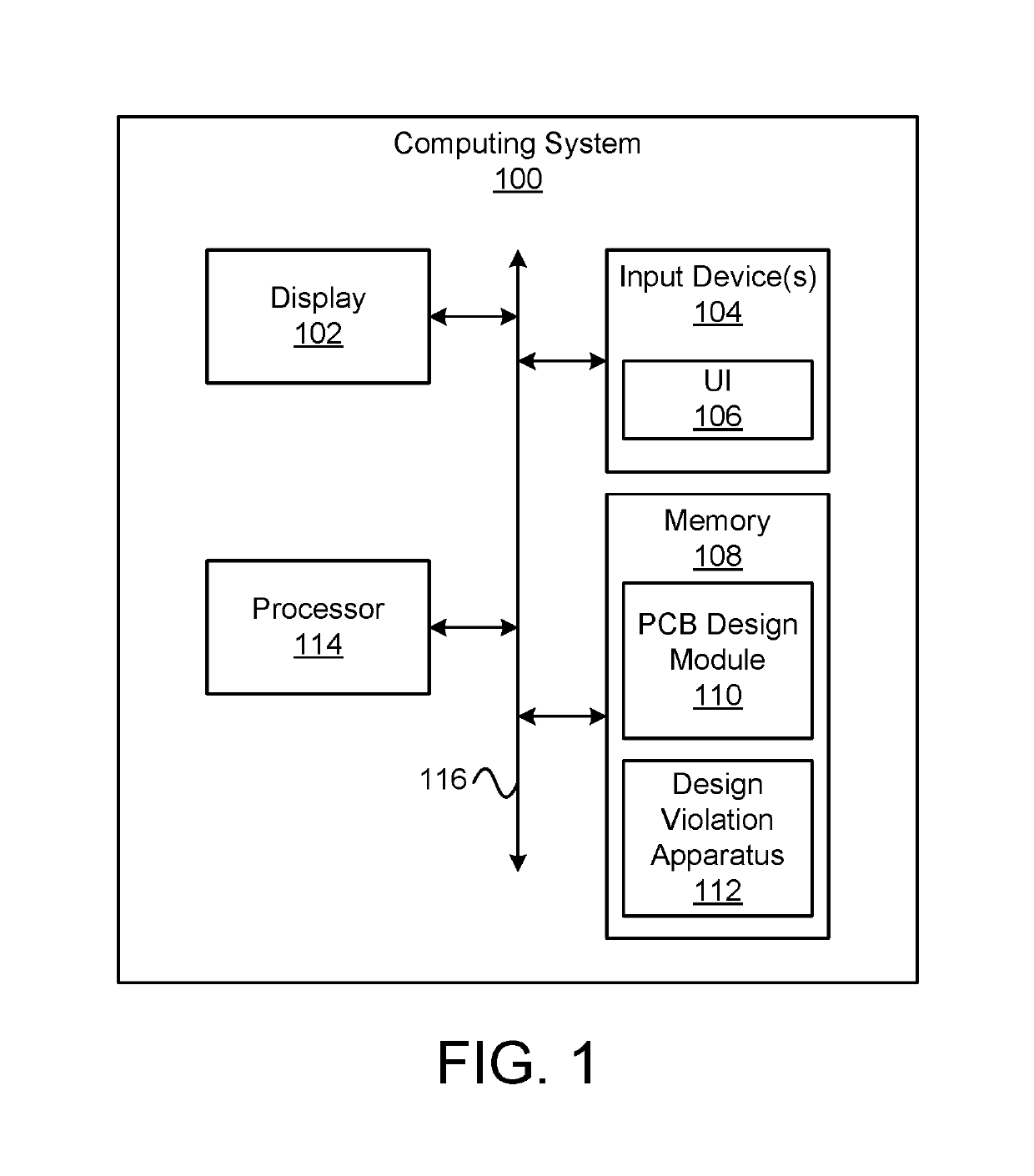
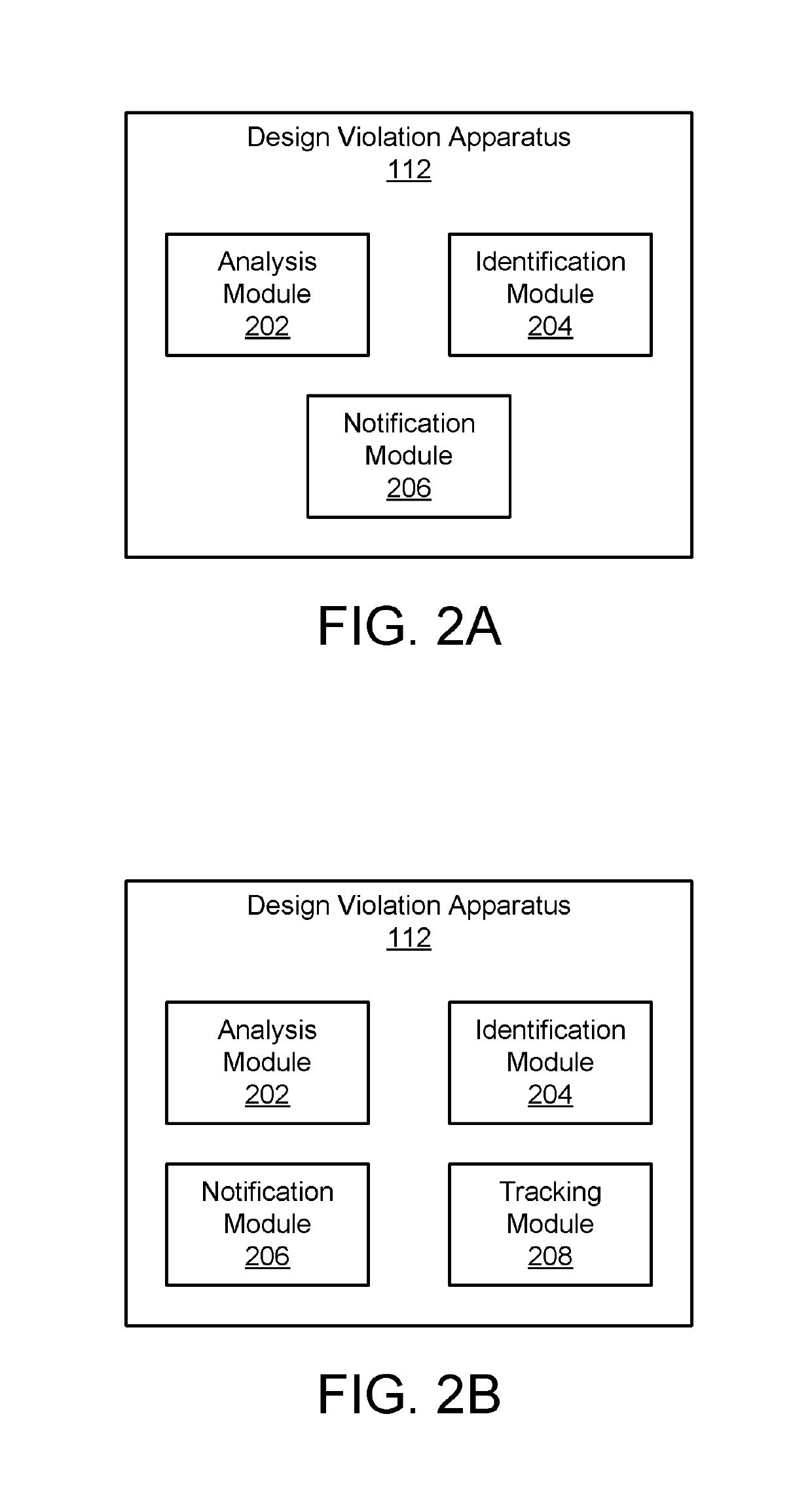
[0085] a PCB design includes a first layer 402 including a first reference voltage, a second layer 404 including a second reference voltage, a third layer 406 (e.g., a trace layer) for including a set of traces (and / or a bus) therein between the first and second layers 402 and 404, and voids 408 separating the first, second, and third layers 402, 404, and 406. While a user is adding a trace or bus to the third layer 406, a tracking module 208 tracks and / or determines the position of an UI 106 (e.g., a cursor). As the cursor adds the trace(s) / bus on the third layer 406, an analysis module 202 analyzes the position(s) / location(s) where the trace / bus is / are being added to determine if the position(s) / location(s) include a voltage, air, a non-conductive material, and / or a material without a voltage property.

[0086]In response to the analysis module 202 determining that one or more positions / locations where the trace(s) / bus is being added (via the location of the cursor) includes a voltag...


PUM


Abstract

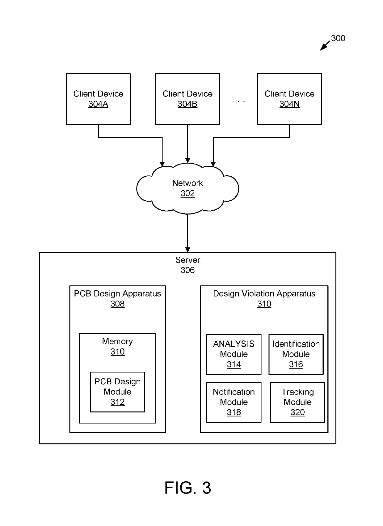
An apparatus for detecting printed circuit board (“PCB”) design violations includes an analysis module that analyzes a position of a trace on a PCB design to determine conductivity of a design material over which the trace is being added and / or an electrical property of the trace at the position. The apparatus further includes an identification module that identifies, in real time, a void violation on the PCB design in response to the design material including a non-conductive material and / or a reference voltage violation on the PCB design in response to the position including a voltage and a notification module that notifies a user of the void violation and / or the reference voltage violation. At least a portion of said modules include hardware circuits, a programmable hardware device, and / or executable code stored on one or more non-transitory computer-readable storage media.

Description

FIELD[0001]The subject matter disclosed herein relates to printed circuit boards (“PCBs”) and more particularly relates to methods and systems for detecting PCB design violations.BACKGROUND[0002]Printed circuit boards (“PCBs”) are commonly used in computing devices. Contemporary PCBs can include several layers separated by voids (e.g., by air, glass, and / or another non-conductive material). Some layers include a reference voltage and other layers include traces. Some designs include alternating trace or bus layers and layers with reference voltages.[0003]Currently, PCBs are designed and prototypes are built prior to determining whether there are flaws in the design. That is, design flaws are typically discovered after a prototype is built and tested. As such, after a flaw is detected in a particular design prototype, a human is typically responsible for discovering / determining the flaw and making design changes to correct the flaw. Discovering / determining design flaws and making des...

Claims


Application Information

Patent Timeline
Patent Type & Authority Patents(United States)
IPC IPC(8): H05K3/00
CPCH05K3/0005G06F30/398
Inventor GARZA, ALBERTOKOWALSKI, EMILE L.MALDONADO, JULIO A.RODRIQUEZ, JOSE L.
Owner IBM CORP
Why Eureka
Try Eureka