Compound, method for manufacturing the compound, and composition for forming organic film

a compound and organic film technology, applied in the field of compound, method for manufacturing the compound, and composition for forming organic film, can solve the problems of not having the inability to produce semiconductor devices in a good yield, and the inability to achieve a complete etching selectivity between the photoresist film and the production process of semiconductor devices, etc., to achieve excellent gap filling/planar

Active Publication Date: 2020-03-31
INT BUSINESS MASCH CORP +1
View PDF42 Cites 1 Cited by
  • Summary
  • Abstract
  • Description
  • Claims
  • Application Information

AI Technical Summary

Benefits of technology

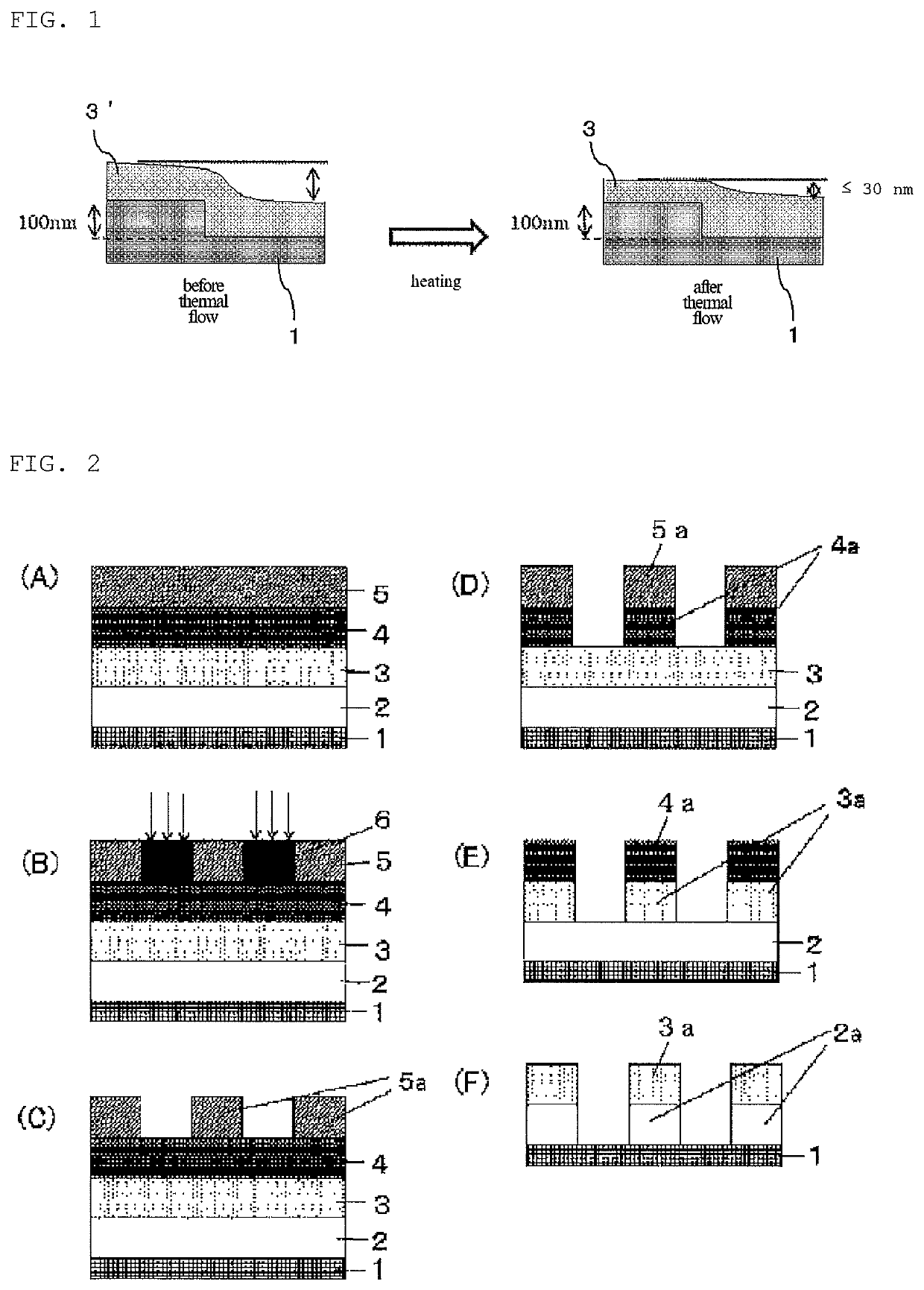
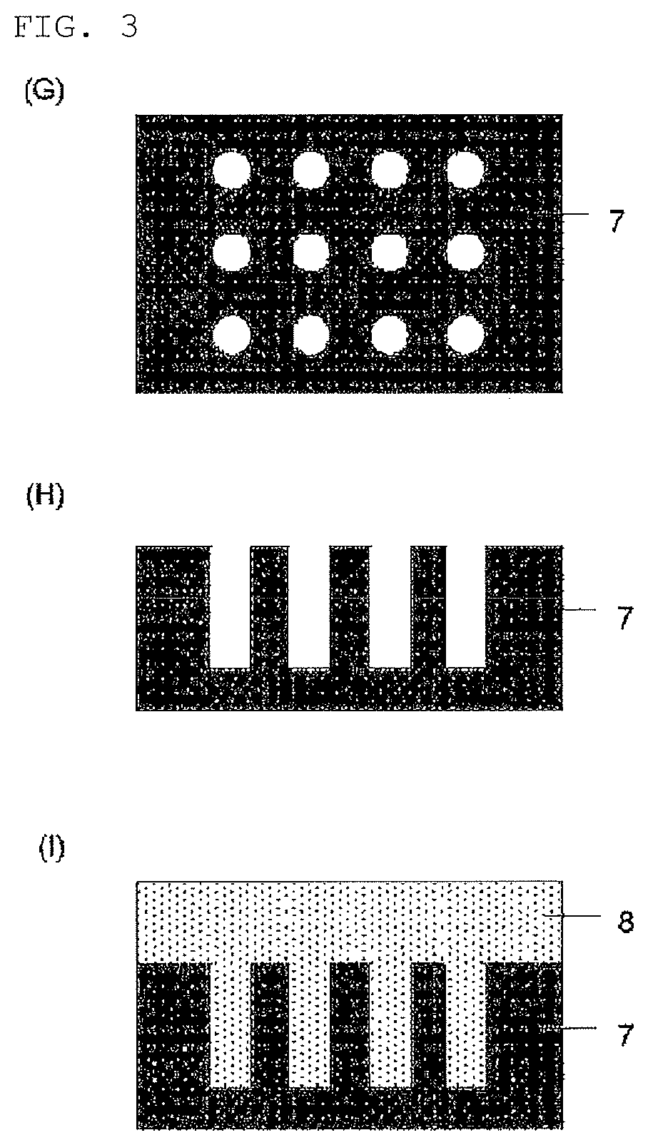
[0050]As described above, the inventive compound is a compound that is curable in film forming in an inert gas, which prevents a substrate from corrosion, without forming volatile byproducts, and is useful for forming an organic under layer film that has higher gap filling and planarizing characteristics. The composition for forming an organic film containing this compound is a material capable of forming an organic film that has excellent gap filling / planarizing characteristics combined with various properties such as heat resistance and etching durability. Accordingly, they are very useful as an organic film material in multilayer resist processes such as a two-layer resist process, a three-layer resist process using a silicon middle layer film, and a four-layer resist process using a silicon middle layer film and an organic bottom antireflective coating as well as a planarization material for producing a semiconductor device. The organic film formed from the inventive composition for forming an organic film is excellent in heat resistance, and is favorably used for patterning without causing fluctuation of the film thicknesses due to thermal decomposition even during CVD (Chemical Vapor Deposition) deposition of hard mask on the organic under layer film.
[0051]Additionally, the method for manufacturing the compound makes it possible to form a skeleton of the compound (polymer) without using a transition metal catalyst.

Problems solved by technology

Practically, however, there is no dry etching method having a complete etching selectivity between the photoresist film and the substrate to be processed.
On the other hand, the attempt to produce smaller pattern sizes in production processes of semiconductor devices is approaching the inherent limit due to the wavelength of a light source for photolithography.
On the other hand, it is difficult to produce semiconductor devices in a good yield by a single layer resist process since it requires an upper layer resist film to have thicker film thickness for gap filling a stepped or patterned substrate to be processed, thereby causing lower tolerance for pattern forming in exposure such as pattern collapse after exposure and development as well as degradation of a pattern profile due to reflection from a substrate in exposure.
This risks the semiconductor device to fail to attain higher processing speed as it is designed, and fail to attain the yield that can be managed as industrial manufacturing.
For these materials, however, the actual curing conditions in an inert gas is not exemplified.

Method used


Image

  • Compound, method for manufacturing the compound, and composition for forming organic film
  • Compound, method for manufacturing the compound, and composition for forming organic film
  • Compound, method for manufacturing the compound, and composition for forming organic film

Examples


synthesis example 1

[Synthesis Example 1] Synthesis of Compound (A1)

[0150]A mixture of 200 g of Diol (B1), 800 g of 1,2-dichloroethene, and 76 g of acetyl chloride was heated to reflux for 72 hours. After cooling to room temperature, 400 mL of diisopropyl ether was added thereto. The yielded solid was filtered off, and dried in vacuum to give 211 g of Dichloride (B2).

[0151]Into an ice-cooled mixture of 10.2 g of ethynylbenzene and 80 g of toluene, 100 mL of 1 N tetrahydrofuran solution of ethylmagnesium bromide was added, and this was allowed to gradually raise the temperature to room temperature. After addition of 13.2 g of Dichloride (B2), this was heated and stirred at 60° C. for 5 hours. After cooling, dilute hydrochloric acid was added to stop the reaction. This was washed with water, followed by concentration in vacuum to give 16.3 g of the object (A1). The following are analytical results of IR and LC-MS for the synthesized Compound (A1).

[0152]

[0153]IR (D-ATR): ν=3285, 3060, 1600, 1490, 1448, 81...

synthesis example 2

[Synthesis Example 2] Synthesis of Compound (A2)

[0155]Compound (A2) was synthesized by the method in accordance with Synthesis Example 1 except for using 1-ethynyl-4-methoxybenzene instead of ethynylbenzene. The following are analytical results of IR and LC-MS for the synthesized Compound (A2).

[0156]

[0157]IR (D-ATR): ν=3037, 2955, 2933, 2835, 1605, 1509, 1448, 1290, 1248, 1170, 1030, 831, 812, 765, 754, and 736 cm−1

[0158]LC-MS (MM-ES Positive / aq.AcONH4-MeCN): m / z=743 (C56H38O2+H+).

synthesis example 3

[Synthesis Example 3] Synthesis of Compound (A3)

[0159]To a mixture of 6.9 g of Dichloride (B2) and 50 g of toluene, 100 mL of 0.5 N tetrahydrofuran solution of ethylmagnesium bromide was added, and this was refluxed with heating for 200 minutes. After cooling, dilute hydrochloric acid was added to stop the reaction. This was washed with water, followed by concentration in vacuum to give 6.6 g of the compound (A3). The weight average molecular weight (Mw) and dispersity (Mw / Mn) were determined by GPC, and found that Mw=1100 and Mw / Mn=1.74. The following are analytical results of IR and 1H NMR for the synthesized Compound (A3).

[0160]

[0161]IR (D-ATR): ν=3291, 3061, 3036, 1604, 1493, 1475, 1448, 1005, 920, 815, 753, 730, and 650 cm−1

[0162]1H NMR (600 MHz, THF-d8) δ (ppm): 2.85-2.90 (2H, HC≡C—), 7.00-7.85 (49H, Ar—H).


PUM

PropertyMeasurementUnit
weight-average molecular weightaaaaaaaaaa
temperatureaaaaaaaaaa

Abstract

A compound includes two or more structures shown by the following general formula (1-1) in the molecule,“Ar” represents an aromatic ring or one that contains at least one nitrogen atom and / or sulfur atom optionally having a substituent, and two Ars are optionally bonded with each other to form a ring structure; the broken line represents a bond with Y; Y represents a divalent or trivalent organic group having 6 to 30 carbon atoms that contains an aromatic ring or a heteroaromatic ring optionally having a substituent, the bonds of which are located in a structure of the aromatic ring or the heteroaromatic ring; R represents a hydrogen atom or a monovalent group having 1 to 68 carbon atoms. This compound can be cured even in an inert gas not only in air atmosphere without forming byproducts, and can form an organic under layer film.

Description

TECHNICAL FIELD[0001]The present invention relates to a compound, a method for manufacturing the compound and a composition for forming an organic film containing the compound that is usable in an inert gas in a process for producing a semiconductor device.BACKGROUND ART[0002]Semiconductor devices have been highly integrated and advanced in processing speed by shifting the wavelength of a light source shorter to attain a finer pattern size in lithography technologies using a light exposure (photolithography) as common arts. In order to form such a fine circuit pattern on a semiconductor device substrate (a substrate to be processed), the substrate is usually processed by dry etching using a photoresist film having a formed pattern as an etching mask. Practically, however, there is no dry etching method having a complete etching selectivity between the photoresist film and the substrate to be processed. Accordingly, substrate processing by a multilayer resist process has been commonl...

Claims


Application Information

Patent Timeline
Patent Type & Authority Patents(United States)
IPC IPC(8): C08F38/00C08G61/02C08K5/00
CPCC08F38/00C08G61/02C08K5/0025C08L2203/16C08G2261/43C08G2261/419C08G2261/1642C08F2500/02C08K5/0016C07C13/567C07C15/02C07C13/62C07C13/66C07D221/16C07D519/00C07C15/50C07C43/21C07C43/285C07D307/91C07D209/86C07D333/08C07D311/82C07D335/12C07C211/55C07C35/38C07C39/225G03F7/004C07C2603/18C07C2603/32C07C2603/24C07D209/82C07D311/80C07D335/10G03F7/094H01L21/0332H01L21/31116H01L21/31138H01L21/31144C07C49/796C07C49/798C07C2/861C07C17/16C07C23/18C07C29/143C07D311/78C07D333/10G03F7/11
Inventor TACHIBANA, SEIICHIROWATANABE, TAKERUNIIDA, KEISUKENAGAI, HIROKOSAWAMURA, TAKASHIOGIHARA, TSUTOMUHESS, ALEXANDER EDWARDBREYTA, GREGORYSANDERS, DANIEL PAULWOJTECKI, RUDY J.
Owner INT BUSINESS MASCH CORP
Why Eureka
Try Eureka