Fabrication of carbon nanoribbons from carbon nanotube arrays
a carbon nanotube and carbon nanotube technology, applied in the direction of graphene nanoribbons, aligned nanotubes, energy-based chemical/physical/physicochemical processes, etc., can solve the problems of power-intensive and incompatibility with various scalable processes
- Summary
- Abstract
- Description
- Claims
- Application Information
AI Technical Summary
Benefits of technology
Problems solved by technology
Method used
Image
Examples
example 1
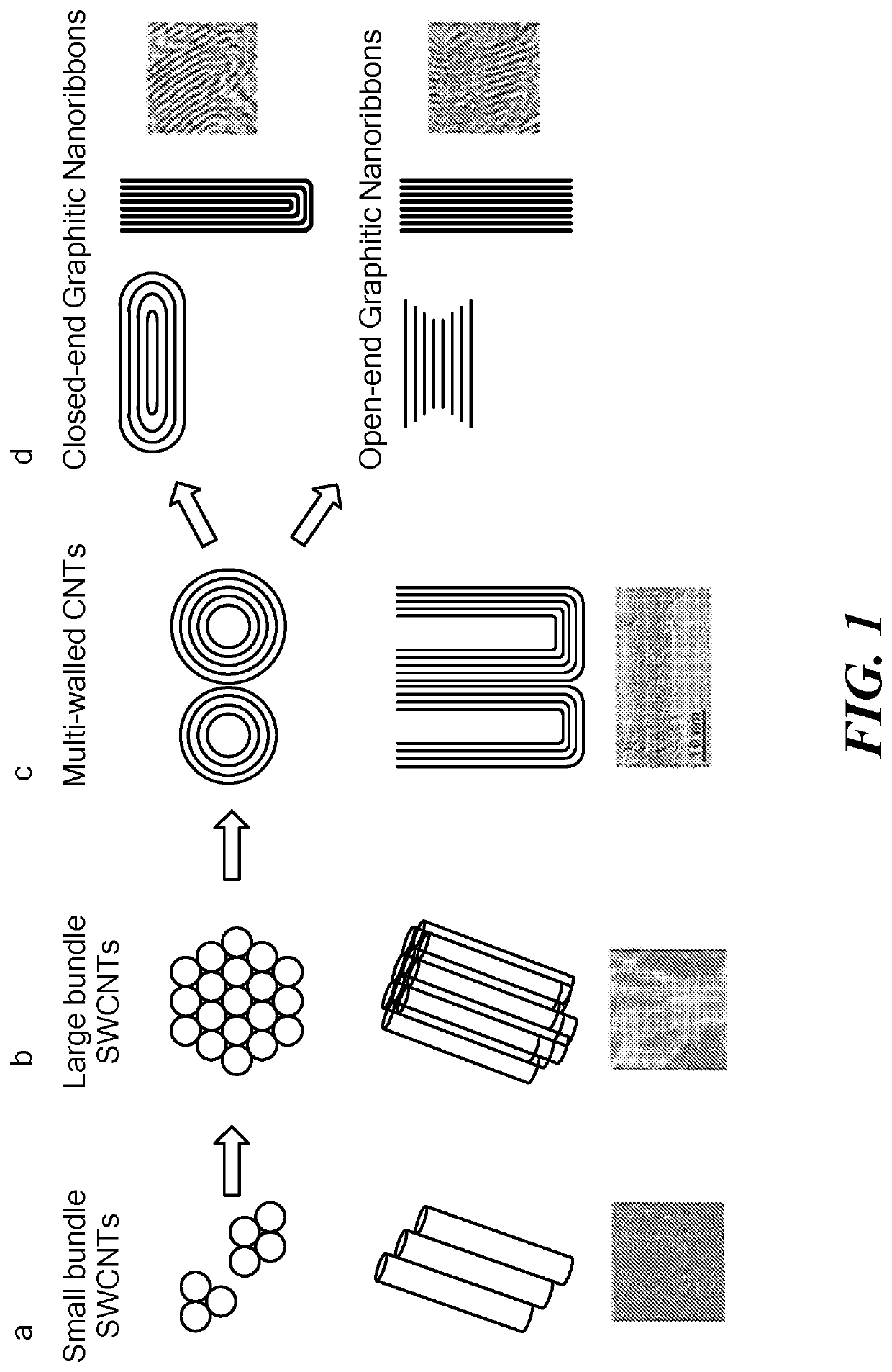
Fabrication of a Highly Aligned SWCNT Network
[0095]One method of preparing an SWCNT network suitable as starting material for a method of the invention is described by way of example. The basic steps for building organized SWCNT lateral architectures fabricated using the template-guided fluidic assembly process (30-32), were as follows. First, a 300-nm-thick polymethyl methacrylate photoresist was deposited on a substrate and baked at 160° C. for 90 s. Second, polymethyl methacrylate patterns were constructed on the substrate using electronbeam lithography to build nanoscale channels, which form templates for building the test architectures and these templates were then developed in the solution (methyl isobutyl ketone / isopropyl alcohol=1:3) for 100 s followed by a 30-s rinse in isopropyl alcohol solution. Next, these template substrates were dip-coated in a 0.23 wt % high-purified SWCNT solution at a constant pulling rate of 0.1 mm / min. The dip-coating processes result in stable an...
example 2
Allotropic Transformation of SWCNT Network
[0098]A Keithley 2,400 sourcemeter was used to apply voltage and to measure the resistance across the two terminal SWCNT devices. All the measurements were done under high vacuum (P−5 Torr) in a Janis Research ST-500 cryogenic probe station to reduce radial heat losses through gas convection and to avoid burning the devices. Voltage sweeps were applied through SWCNT arrays to find the breakdown voltage. Most of the arrays failed at a maximum current density of about 4.3×10⁷ A / cm2, and the breakdown voltage (Vb) was 2.7V on the TEM window (FIG. 4B). By sweeping the voltage over a suitable range, a critical voltage was observed for which the graphitization process was accelerated. At the same time, applied voltages too close to Vb often led to the breakdown of the nanotube. Therefore, Vb for these quasiparallel SWCNT networks was found to be an important parameter.
[0099]The Vb in fabricated devices could be predicted statistically by Vb=−2.14 ...
example 3
Temperature by Electrical Energy
[0101]Breakdown occurs when the maximum temperature of the tube reaches the value of the breakdown temperature, which allows the extraction of a simple expression for the breakdown voltage of SWCNTs, including heat generation from Joule self-heating and heat loss to the substrate (50,51).
VBD=gL(TBD−T0) / IBD+IBDRC
Therefore, the maximum temperature at the breakdown voltage is:
TBD=(PBD−I2BDRC) / gL+T0
Here, TBD is the maximum temperature, PBD is the breakdown power, the combined resistance of the source and drain contacts, RC is estimated from the inverse slope of the low-bias ID−VSD plot, RC≈(dID / dVSD)−1, g is the heat dissipation coefficient in the substrate per unit length and L is length of SWCNT network. From the equation, the calculated maximum temperature is about 1,335 K (1,062 C). At 0.8Vb, the temperature is calculated as about 1,200 K.
PUM
| Property | Measurement | Unit |
|---|---|---|
| frequency | aaaaa | aaaaa |
| temperature | aaaaa | aaaaa |
| temperature | aaaaa | aaaaa |
Abstract
Description
Claims
Application Information


