

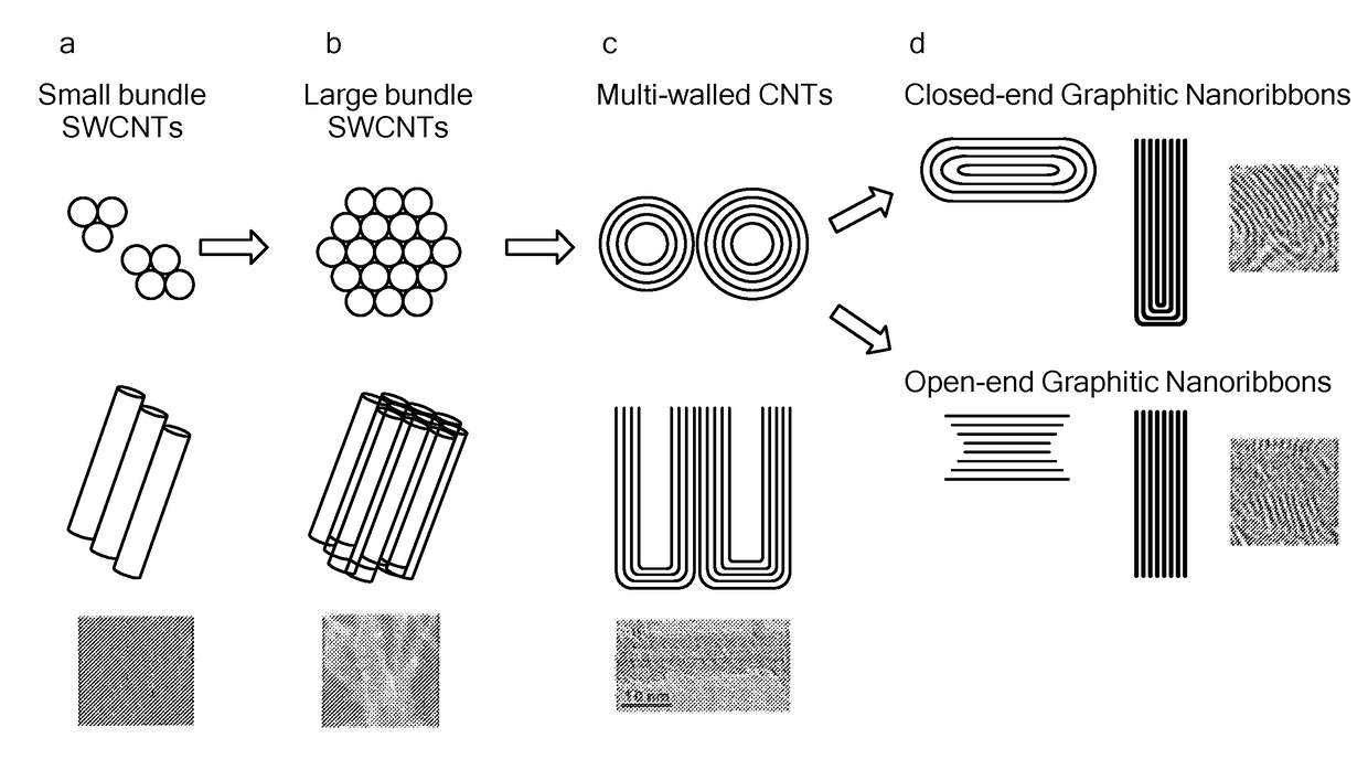
Fabrication of Carbon Nanoribbons from Carbon Nanotube Arrays
a carbon nanotube and carbon nanotube technology, applied in the direction of graphene nanoribbons, aligned nanotubes, energy-based chemical/physical/physicochemical processes, etc., can solve the problems of power-intensive and incompatibility with various scalable processes
- Summary
- Abstract
- Description
- Claims
- Application Information
AI Technical Summary
Benefits of technology
Problems solved by technology
Method used
Image

Examples
example 2
Allotropic Transformation of SWCNT Network
[0098]A Keithley 2,400 sourcemeter was used to apply voltage and to measure the resistance across the two terminal SWCNT devices. All the measurements were done under high vacuum (P−5 Torr) in a Janis Research ST-500 cryogenic probe station to reduce radial heat losses through gas convection and to avoid burning the devices. Voltage sweeps were applied through SWCNT arrays to find the breakdown voltage. Most of the arrays failed at a maximum current density of about 4.3×10⁷ A / cm2, and the breakdown voltage (Vb) was 2.7V on the TEM window (FIG. 4B). By sweeping the voltage over a suitable range, a critical voltage was observed for which the graphitization process was accelerated. At the same time, applied voltages too close to Vb often led to the breakdown of the nanotube. Therefore, Vb for these quasiparallel SWCNT networks was found to be an important parameter.
[0099]The Vb in fabricated devices could be predicted statistically by Vb=−2.14 ...
example 3
Temperature by Electrical Energy
[0101]Breakdown occurs when the maximum temperature of the tube reaches the value of the breakdown temperature, which allows the extraction of a simple expression for the breakdown voltage of SWCNTs, including heat generation from Joule self-heating and heat loss to the substrate (50,51).
VBD=gL(TBD−T0) / IBD+IBDRC
Therefore, the maximum temperature at the breakdown voltage is:
TBD=(PBD−I2BDRC) / gL+T0
Here, TBD is the maximum temperature, PBD is the breakdown power, the combined resistance of the source and drain contacts, RC is estimated from the inverse slope of the low-bias ID−VSD plot, RC≈(dID / dVSD)−1, g is the heat dissipation coefficient in the substrate per unit length and L is length of SWCNT network. From the equation, the calculated maximum temperature is about 1,335 K (1,062 C). At 0.8Vb, the temperature is calculated as about 1,200 K.
example 4
SEM and TEM Observations
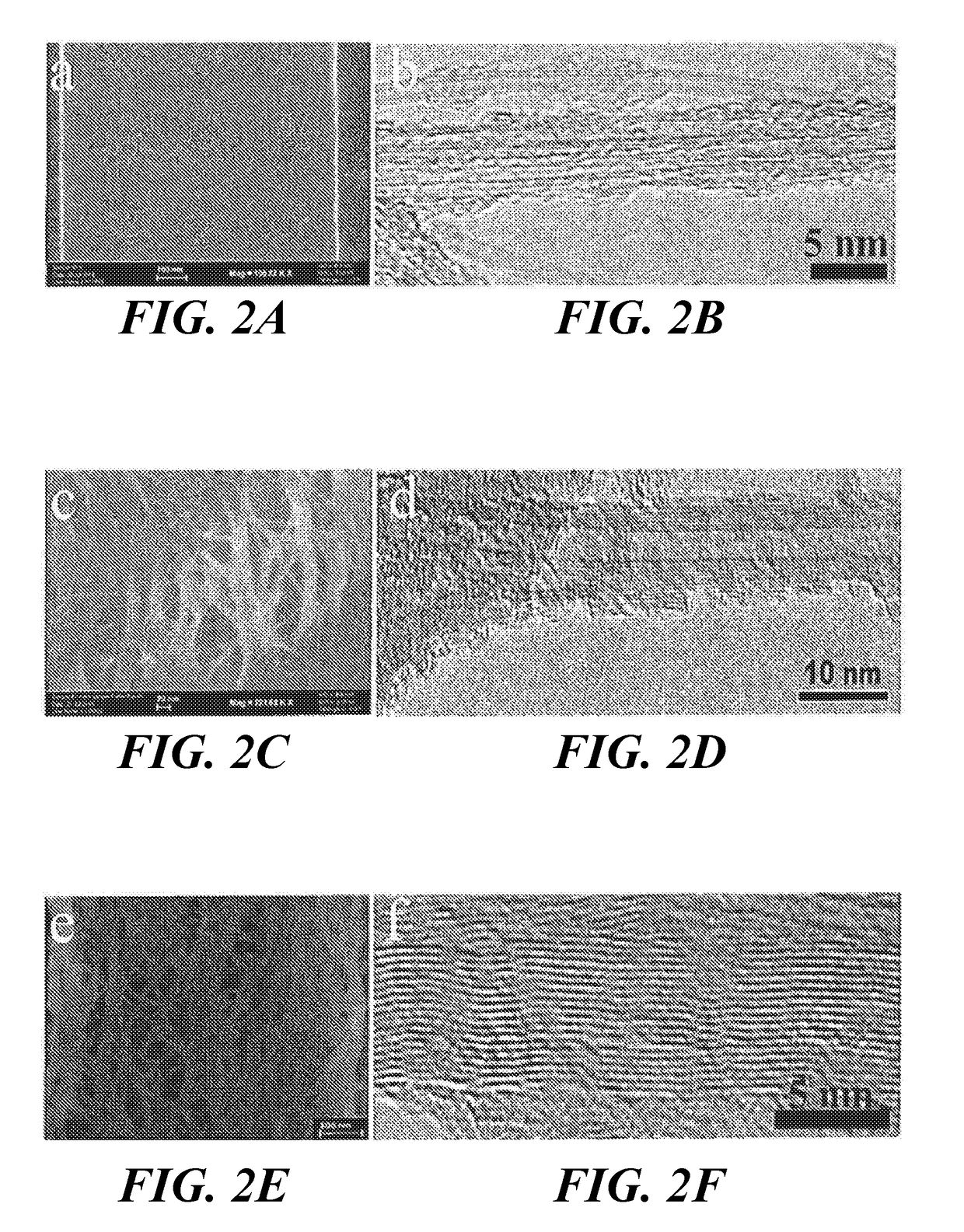
[0102]The SWCNT arrays were prepared on specially designed chips with a window of 40×40 μm2 for SEM and TEM imaging. The SWCNT arrays were suspended on an electron transparent window by employing a two-probe device architecture. Two micro-heater electrodes of 10 μm in width were employed around the arrays on the chip for the external heating. The TEM measurements were carried out in a JEOL-3011 high-resolution TEM instrument using an accelerating voltage of 300 kV. The allotropes covered a significant area of the devices, which was verified by taking TEM images at different positions over the sample.
PUM
 Abstract
Description
Claims
Application Information