Elastic wave device

a wave device and elastic wave technology, applied in the direction of impedence networks, electrical apparatus, transmission, etc., can solve the problems of large power applied, electrical characteristics of reception filters deterioration, etc., and achieve the effect of reducing or preventing the deterioration of electrical characteristics due to noise and deterioration of electrical characteristics

Active Publication Date: 2020-12-08
MURATA MFG CO LTD
View PDF17 Cites 4 Cited by
  • Summary
  • Abstract
  • Description
  • Claims
  • Application Information

AI Technical Summary

Benefits of technology

[0021]Preferred embodiments of the present invention provide elastic wave devices in each of which a deterioration of electrical characteristics or an occurrence of a breakdown due to heat generation is reduced or prevented, and a deterioration of electrical characteristics due to noise is reduced or prevented.
[0024]In this case, the high-thermal-conductivity conductor layer preferably includes a region separated into a region corresponding to the transmission functional electrode and a region corresponding to the reception functional electrode, in the other main surface of the piezoelectric substrate. Generally, in an elastic wave element that is a duplexer or a multiplexer, large power is applied to a transmission functional electrode, and thus, heat is considerably generated in the transmission functional electrode in many cases. On the other hand, large power is not applied to a reception functional electrode, such that not much heat is generated in the reception functional electrode. When the heat generated in the transmission functional electrode is transmitted to the reception functional electrode, a temperature shift occurs in the electrical characteristics of a reception filter, and thus, there is a possibility that the electrical characteristics of the reception filter deteriorate. Therefore, it is preferable that the high-thermal-conductivity conductor layer is separated into the region corresponding to the transmission functional electrode and the region corresponding to the reception functional electrode, and the heat generated in the transmission functional electrode is reduced or prevented from being transmitted to the reception functional electrode via the high-thermal-conductivity conductor layer, such that it is possible to reduce or prevent the function of the reception functional electrode from deteriorating and to reduce or prevent the electrical characteristics of the reception filter from deteriorating.
[0025]In this case, furthermore, the high-thermal-conductivity conductor layer provided in the region corresponding to the transmission functional electrode and the ground terminal provided near the transmission functional electrode are preferably connected to each other by the conductor via. As described above, generally, in an elastic wave element that is a duplexer or a multiplexer, large power is applied to a transmission functional electrode, and thus, heat is considerably generated in the transmission functional electrode in many cases. Therefore, it is preferable for the ground terminal provided near the transmission functional electrode and the high-thermal-conductivity conductor layer to be connected to each other by the conductor via as described above, since it is possible to efficiently dissipate heat generated near the transmission functional electrode, by the conductor via.
[0026]In addition, the high-thermal-conductivity conductor layer provided in the region corresponding to the reception functional electrode and the ground terminal provided near the reception functional electrode are preferably connected to each other by the conductor via. Generally, in an elastic wave element that is a duplexer or a multiplexer, since the SN ratio of a reception signal is lower than that of a transmission signal, electrical characteristics deteriorate more greatly when a reception functional electrode (reception filter) receives noise, than when a transmission functional electrode (transmission filter) receives noise, which becomes a serious problem. Therefore, it is preferable for the high-thermal-conductivity conductor layer provided in the region corresponding to the reception functional electrode and the ground terminal provided near the reception functional electrode to be connected to each other by the conductor via, since it is possible to connect the high-thermal-conductivity conductor layer provided in the region corresponding to the reception functional electrode to ground and to perform shielding, and further, it is possible to effectively protect the reception functional electrode (reception filter) from noise to reduce or prevent deterioration of electrical characteristics due to noise.
[0028]In elastic wave devices according to preferred embodiments of the present invention, since the conductor via penetrates between both main surfaces of the elastic wave element, and the high-thermal-conductivity conductor layer and the ground terminal are electrically connected to each other by the conductor via, a deterioration of electrical characteristics and / or an occurrence of a breakdown due to heat generation is reduced or prevented, and a deterioration of electrical characteristics due to noise is reduced or prevented.

Problems solved by technology

On the other hand, large power is not applied to a reception functional electrode, such that not much heat is generated in the reception functional electrode.
When the heat generated in the transmission functional electrode is transmitted to the reception functional electrode, a temperature shift occurs in the electrical characteristics of a reception filter, and thus, there is a possibility that the electrical characteristics of the reception filter deteriorate.

Method used


Image

  • Elastic wave device
  • Elastic wave device
  • Elastic wave device

Examples


first preferred embodiment

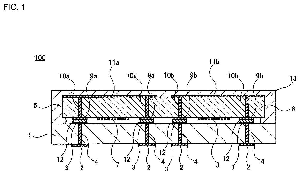
[0042]FIG. 1 shows an elastic wave device 100 according to a first preferred embodiment of the present invention.

[0043]The elastic wave device 100 includes a substrate 1. For example, a ceramic material is preferably used for the substrate 1. However, the material of the substrate 1 is not particularly limited, and the substrate 1 may be produced from a glass ceramic material, a resin, or other suitable material, for example, instead of the ceramic material. Alternatively, the substrate 1 may have a multilayer structure. In such a case, for example, a high acoustic-velocity support substrate, a low acoustic-velocity film, and a piezoelectric layer are preferably laminated in that order. A high acoustic-velocity support substrate may include a high acoustic-velocity film and a support substrate.

[0044]Outer electrodes 2 are provided on one main surface (the lower main surface in the drawing) of the substrate 1. In addition, first mounting electrodes 3 and second mounting electrodes (n...

second preferred embodiment

[0076]FIG. 5 shows an elastic wave device 200 according to a second preferred embodiment of the present invention.

[0077]Specifically, FIG. 5 is a cross-sectional view of the elastic wave device 200.

[0078]In the elastic wave device 200, the configuration of the elastic wave device 100 according to the first preferred embodiment is partially changed. Specifically, in the elastic wave device 100, the high-thermal-conductivity conductor layers 11a and 11b are buried in the exterior resin layer 13. In the elastic wave device 200, high-thermal-conductivity conductor layers 21a and 21b are externally exposed from the upper main surface of an exterior resin layer 23 by reducing the thickness of the exterior resin layer 23. The remaining configuration of the elastic wave device 200 is the same or substantially the same as that of the elastic wave device 100.

[0079]The high-thermal-conductivity conductor layers 21a and 21b of the elastic wave device 200 have a better heat dissipating effect th...

third preferred embodiment

[0080]FIG. 6 shows an elastic wave device 300 according to a third preferred embodiment of the present invention. Specifically, FIG. 6 is a cross-sectional view of the elastic wave device 300.

[0081]In the elastic wave device 300, the configuration of the elastic wave device 200 according to the second preferred embodiment is partially changed. Specifically, in the elastic wave device 300, the areas of the high-thermal-conductivity conductor layers 21a and 21b of the elastic wave device 200 are increased and the high-thermal-conductivity conductor layers 21a and 21b are replaced by high-thermal-conductivity conductor layers 31a and 31b, respectively. The high-thermal-conductivity conductor layer 31a is extended leftward in FIG. 6 to the upper left edge of the exterior resin layer 23. Similarly, the high-thermal-conductivity conductor layer 31b is extended rightward in FIG. 6 to the upper right edge of the exterior resin layer 23.

[0082]In the elastic wave device 300, the high-thermal-...


PUM

PropertyMeasurementUnit
thermal-conductivityaaaaaaaaaa
thermal conductivityaaaaaaaaaa
elastic waveaaaaaaaaaa

Abstract

An elastic wave device includes a substrate, an elastic wave element, and an exterior resin layer. The substrate includes an outer electrode on one main surface thereof and a first mounting electrode on another main surface thereof. The elastic wave element includes a piezoelectric substrate, a transmission functional electrode, a reception functional electrode, and ground terminals on one main surface of the piezoelectric substrate, and the ground terminals are connected to the first mounting electrode. High-thermal-conductivity conductor layers are provided on another main surface of the piezoelectric substrate, conductor vias penetrate between both main surfaces of the piezoelectric substrate, and the high-thermal-conductivity conductor layers and the ground terminals are connected to each other by the conductor vias.

Description

CROSS REFERENCE TO RELATED APPLICATIONS[0001]This application claims the benefit of priority to Japanese Patent Application No. 2016-129077 filed on Jun. 29, 2016 and is a Continuation Application of PCT Application No. PCT / JP2017 / 023651 filed on Jun. 27, 2017. The entire contents of each application are hereby incorporated herein by reference.BACKGROUND OF THE INVENTION1. Field of the Invention[0002]The present invention relates to an elastic wave device.2. Description of the Related Art[0003]Elastic wave devices have been used as high-frequency signal transmitting / receiving components in portable terminal devices or the like. In some cases, large power is applied to the elastic wave device. In such a case, heat is generated in a piezoelectric substrate or a functional electrode (IDT electrode). If the generated heat remains in the elastic wave device, the efficiency of output power with respect to input power may decrease. In addition, the electrical characteristics of the elastic...

Claims


Application Information

Patent Timeline
Patent Type & Authority Patents(United States)
IPC IPC(8): H03H9/64H03H3/08H03H9/02H03H9/145H03H9/25H03H9/10H03H9/05H04B1/38H03H9/08H03H9/72
CPCH04B1/38H03H9/6489H03H9/1078H03H9/25H03H9/0576H03H9/725H03H3/08H03H9/1085H03H9/145H03H9/059H03H9/02559H03H9/02913H03H9/08
Inventor FUJIYA, MASAHARUWATANABE, KAZUSHI
Owner MURATA MFG CO LTD
Why Eureka
Try Eureka