Display device including photo pixel with improved sensing sensitivity

a technology of sensing sensitivity and display device, which is applied in the field of display device including light sensing area, can solve the problems of increasing costs while sensitivity, and achieve the effect of increasing costs

Active Publication Date: 2021-03-23
SAMSUNG DISPLAY CO LTD
View PDF56 Cites 0 Cited by
  • Summary
  • Abstract
  • Description
  • Claims
  • Application Information

AI Technical Summary

Benefits of technology

[0004]In an optical type using an optical sensor, a separate modular optical sensor is disposed (e.g., mounted) in a display device, so that it raises costs while sensitivity does not reach a level at which a fingerprint of a user is sensed.
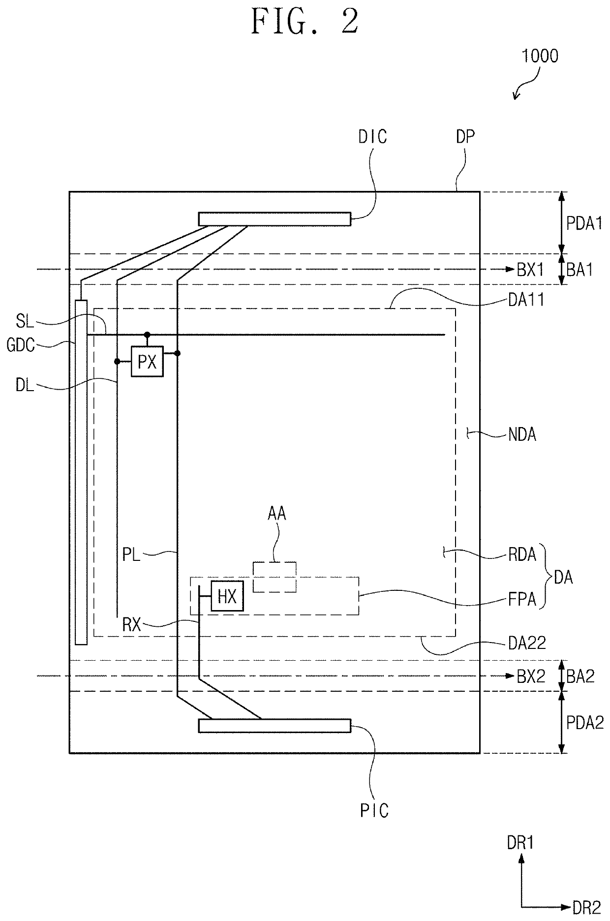
[0006]Exemplary embodiments of the invention also provide a display device that does not change the arrangement structure of display elements even when photo pixel areas are provided in a light sensing area and thus maintains a constant resolution in a display area regardless of the area.

Problems solved by technology

In an optical type using an optical sensor, a separate modular optical sensor is disposed (e.g., mounted) in a display device, so that it raises costs while sensitivity does not reach a level at which a fingerprint of a user is sensed.

Method used


Image

  • Display device including photo pixel with improved sensing sensitivity
  • Display device including photo pixel with improved sensing sensitivity
  • Display device including photo pixel with improved sensing sensitivity

Examples


Embodiment Construction

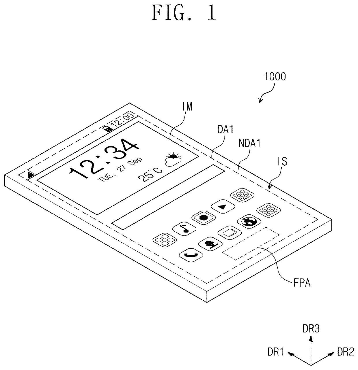
[0045]Hereinafter, another exemplary embodiment of the invention will be described with reference to the drawings. In this specification, when it is mentioned that a component (or, an area, a layer, a part, etc.) is referred to as being “on”, “connected to” or “combined to” another component, this means that the component may be directly on, connected to, or combined to the other component or a third component therebetween may be present.

[0046]Like reference numerals refer to like elements. Additionally, in the drawings, the thicknesses, proportions, and dimensions of components are exaggerated for effective description. “And / or” includes all of one or more combinations defined by related components.

[0047]It will be understood that the terms “first” and “second” are used herein to describe various components but these components should not be limited by these terms. The above terms are used only to distinguish one component from another. For example, a first component may be referre...


PUM

PropertyMeasurementUnit
DAaaaaaaaaaa
DAaaaaaaaaaa
distanceaaaaaaaaaa

Abstract

A display device includes a substrate, a driving layer which is disposed on the substrate, and includes first driving circuit groups each including N first pixel driving circuits and photo pixels each including a photo driving circuit and a photo sensor electrically connected to the photo driving circuit. A display element layer is on the driving layer, and includes first display element groups each including N first display elements electrically connected to the respective N first pixel driving circuits. Minimum distances between first color display elements included in the first display elements in a first predetermined direction in a plan view, are substantially the same. A distance between two first pixel driving circuits adjacent to each other in a second predetermined direction with the photo pixel therebetween in the plan view is different from a distance between two first pixel driving circuits continuously disposed in the second predetermined direction.

Description

[0001]This application claims priority to Korean Patent Application No. 10-2017-0099204, filed on Aug. 4, 2017, and all the benefits accruing therefrom under 35 U.S.C. § 119, the content of which in its entirety is herein incorporated by reference.BACKGROUND1. Field[0002]Exemplary embodiments of the invention relate to a display device, and more particularly to a display device including a light sensing area.2. Description of the Related Art[0003]Recently, display devices have a function for sensing user's fingerprints. Examples of a fingerprint recognition method include an electrostatic capacity type based on a change in capacitance of a capacitor formed between electrodes, an optical type using an optical sensor, and an ultrasonic type using a piezoelectric body.SUMMARY[0004]In an optical type using an optical sensor, a separate modular optical sensor is disposed (e.g., mounted) in a display device, so that it raises costs while sensitivity does not reach a level at which a finge...

Claims


Application Information

Patent Timeline
Patent Type & Authority Patents(United States)
IPC IPC(8): G09G5/00H01L27/32G09G3/3225G06K9/00G06F3/044H01L51/00
CPCH01L27/3234G06K9/0004G09G3/3225G06F3/044G09G2360/14H01L27/323H01L27/3246H01L51/0097G06V40/13H10K59/40H10K59/65H10K59/122H10K77/111G06V40/1318
Inventor JUNG, KEUMDONG
Owner SAMSUNG DISPLAY CO LTD
Why Eureka
Try Eureka