
Lighting device and inspection apparatus having the same

a technology of inspection apparatus and light source, which is applied in the direction of photomechanical apparatus, instruments, material analysis through optical means, etc., can solve the problem that the high fps camera tends to generate images with a relatively large shot nois

Active Publication Date: 2022-04-26
SAMSUNG ELECTRONICS CO LTD
View PDF13 Cites 0 Cited by
  • Summary
  • Abstract
  • Description
  • Claims
  • Application Information

AI Technical Summary

Problems solved by technology

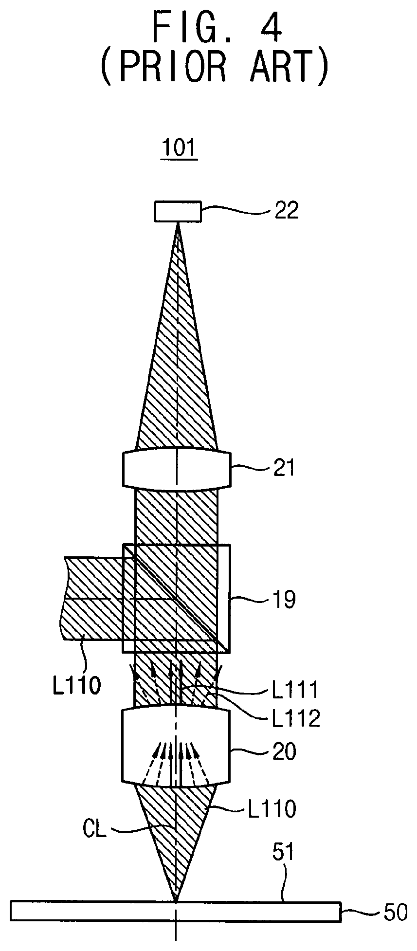
However, the conventional halogen lamp and LED produce illumination light of such small luminance that the high fps camera tends to generate images having a relatively large shot noise.

Method used


Image

  • Lighting device and inspection apparatus having the same
  • Lighting device and inspection apparatus having the same
  • Lighting device and inspection apparatus having the same

Examples


Embodiment Construction

[0021]Examples of the present inventive concept will now be described in detail with reference to the accompanying drawings, wherein like reference numerals designate like components throughout.

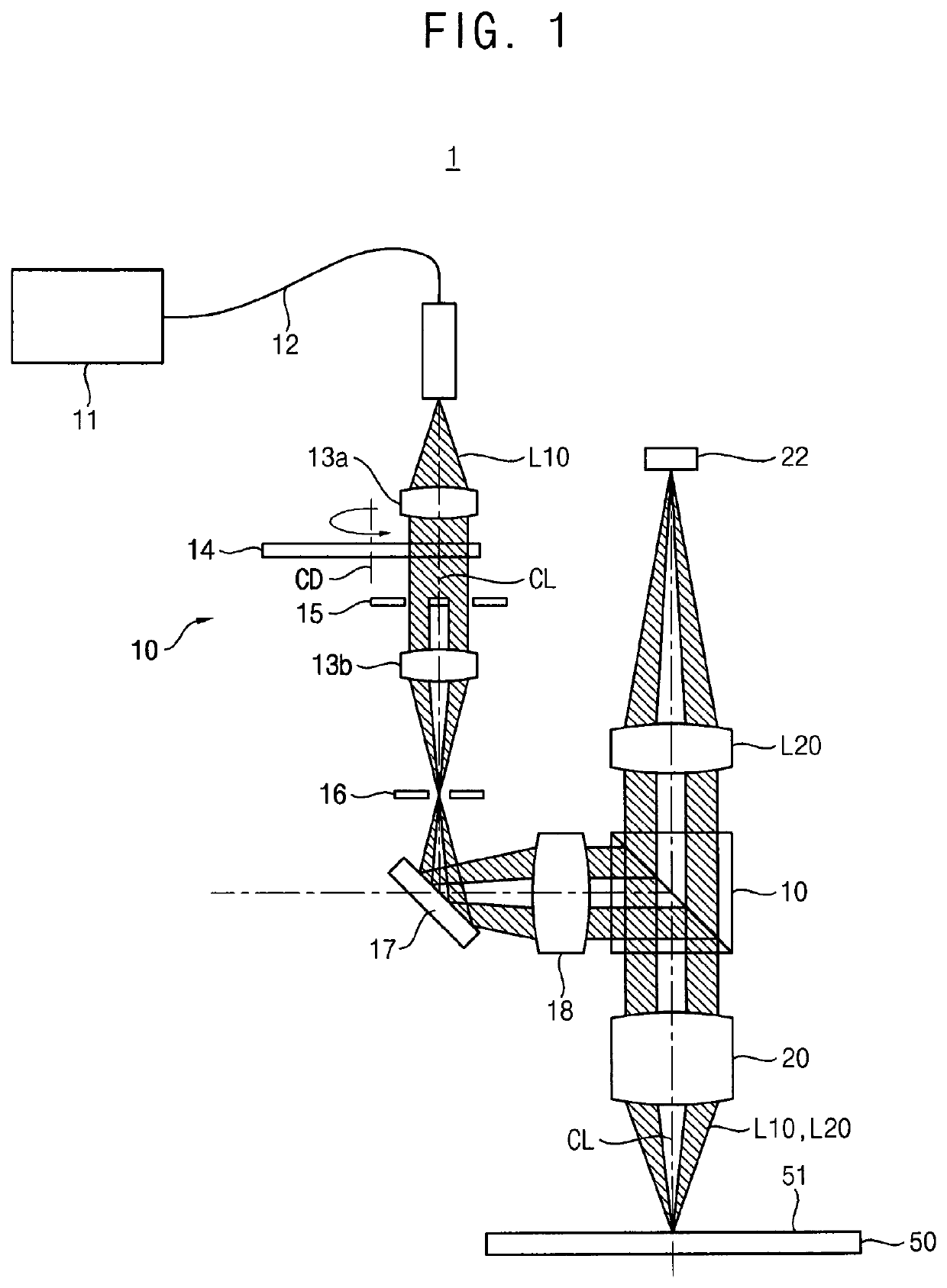
[0022]FIG. 1 illustrates a first example of an inspection apparatus in accordance with the present inventive concept. In the present example, the inspection apparatus may inspect a semiconductor wafer on which at least a semiconductor process has been conducted.

[0023]Referring to FIG. 1, the inspection apparatus 1 may include a lighting device 10 for emitting an illumination light L10 to illuminate a wafer under inspection (WUI) 50. At first, the structure of the lighting device 10 will be described in detail and then the structure and operation of the inspection apparatus 1 will be described in detail hereinafter.

[0024]

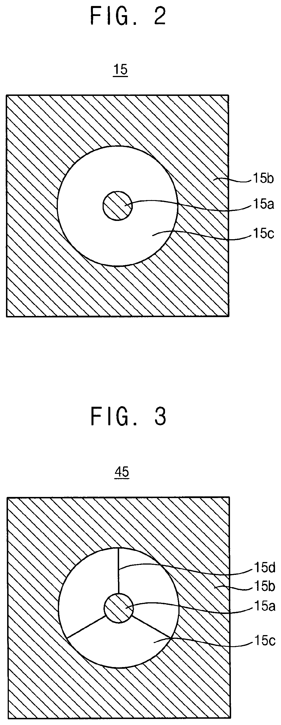
[0025]As shown in FIG. 1, the lighting device 10 may include a light source 11, an optical fiber 12, a collimator lens 13a, a focus lens 13b, a light phase modulator 14, an ap...


PUM

PropertyMeasurementUnit
transmittanceaaaaaaaaaa
phaseaaaaaaaaaa
optical pathaaaaaaaaaa

Abstract

A lighting device includes a light source generating a beam of illumination light, a ring-shaped aperture shielding a central portion of the illumination light and transforming the beam of illumination light into ring-shaped illumination light, and an object lens focusing the ring-shaped illumination light such that a specimen can be illuminated with the ring-shaped illumination light. An inspection apparatus including the light device also has a beam splitter and an image sensor picking up light reflected and / or diffracted from the specimen through the beam splitter. Because a central portion of the illumination light is shielded, lens flare of light transmitted by the beam splitter and the object lens is prevented thereby preventing speckles in the image produced by the image sensor.

Description

PRIORITY STATEMENT[0001]This application claims priority under 35 U.S.C § 119 to Japan Patent Application No. 2018-202969 filed on Oct. 29, 2018 in the Japan Intellectual Property Office and Korean Patent Application No. 10-2018-0163949 filed on Dec. 18, 2018 in the Korean Intellectual Property Office, the disclosure of which is hereby incorporated by reference in its entirety.BACKGROUND1. Field[0002]The present inventive concept relates to a lighting device and an inspection apparatus including the same. More particularly, the inventive concept relates to a lighting device comprising a laser for generating illumination light and an inspection apparatus having such a lighting device for inspecting semiconductor wafers.2. Description of the Related Art[0003]An inspection apparatus for inspecting semiconductor wafers (referred to as a wafer inspection apparatus) using a high resolution camera and a high magnification lens can detect features of chips on the wafer on a scale of nanomet...

Claims


Application Information

Patent Timeline
Patent Type & Authority Patents(United States)
IPC IPC(8): G02B21/08G02B21/36G02B26/06
CPCG02B21/084G02B21/36G02B26/06G02B21/0016G02B21/14G03F7/70616G01N21/9501G01N21/8806
Inventor HIDAKA, YASUHIROKAJINAMI, MASATOSASAOKA, TAKAYUKI
Owner SAMSUNG ELECTRONICS CO LTD
Learn More