Supercharge Your Innovation With Domain-Expert AI Agents!

Device and method for detecting defect of optical film

a technology of optical film and detection method, which is applied in the field of optical film detection device and detection method, can solve the problems of optical film crushing, optical film stabbery, and various shape defects in/on the optical film, and achieve the effect of widening a region, easy detection of defects existing, and widening a region

Active Publication Date: 2022-07-19
SHANJIN OPTOELECTRONICS (NANJING) CO LTD
View PDF10 Cites 0 Cited by
  • Summary
  • Abstract
  • Description
  • Claims
  • Application Information

AI Technical Summary

Benefits of technology

[0011]According to an exemplary embodiment of the present invention, it is possible to easily detect defects having various shapes such as crushed, stabbed, folded, and wrinkled shapes in / on the optical film.
[0012]According to an exemplary embodiment of the present invention, since the light irradiation width of the light emitted from the light emitting unit is expanded by the reflection unit, it is possible to widen a region in which a defect of the optical film can be detected.
[0013]According to an exemplary embodiment of the present invention, it is possible to easily detect a defect existing in / on the optical film.

Problems solved by technology

During a process of manufacturing and transporting the optical film, defects having various shapes can occur in / on the optical film in certain situations such as when foreign substances are introduced into the optical film, the optical film is crushed, a surface of the optical film is stabbed, or the optical film is wrinkled.
The aforementioned defects can cause defects of display units manufactured by using the optical film.

Method used


Image

  • Device and method for detecting defect of optical film
  • Device and method for detecting defect of optical film
  • Device and method for detecting defect of optical film

Examples


example 1

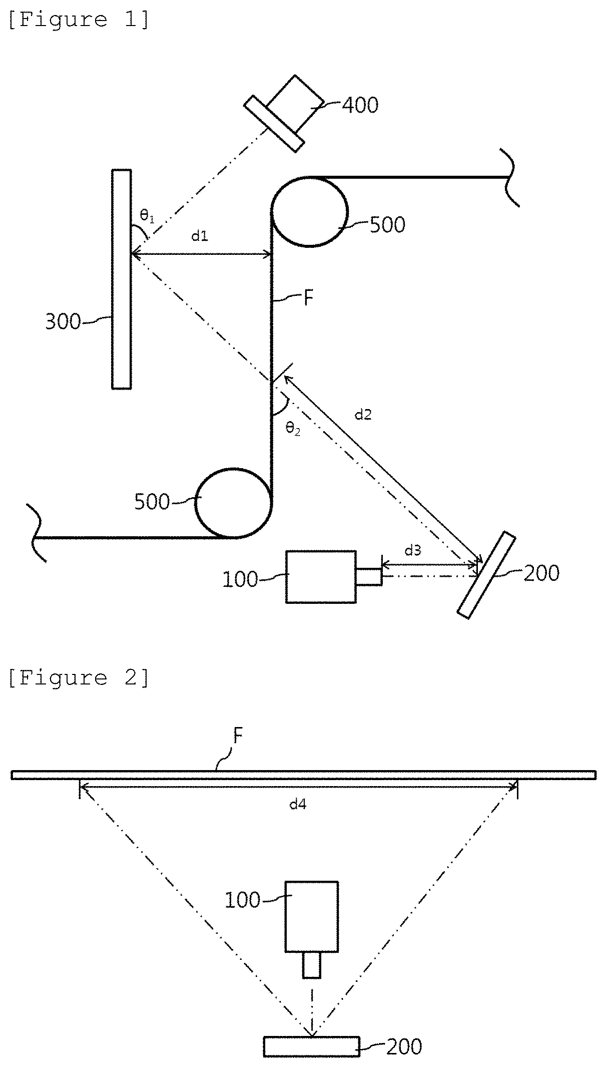
[0078]The light emitting unit, the reflection unit, the screen, the image capturing unit, and the conveying unit of the device for detecting a defect of an optical film were set as illustrated in FIG. 1. In this case, the first angle θ1 and the second angle θ2 were set to 35°. In addition, the distance d1 between the screen and the region of the optical film to which the light is projected was set to 90 mm, the distance d3 between the point on the light emitting unit at which the light is emitted and the point on the reflection unit at which the light is reflected was set to 175 mm, and the distance d2 between the point on the reflection unit at which the light is reflected and the region of the optical film to which the light reflected by the reflection unit is guided was set to 650 mm. In addition, the conveying rollers having a diameter of 118 mm were used, and a shortest distance between the centers of the two conveying rollers in FIG. 1 was set to 245 mm.


PUM

PropertyMeasurementUnit
angleaaaaaaaaaa
angleaaaaaaaaaa
distanceaaaaaaaaaa

Abstract

Provided is a device for detecting a defect of an optical film, comprising a light emitting unit, a reflection unit, a screen, and an image capturing unit, and a method for detecting a defect of an optical film, comprising emitting light to a reflection unit, projecting the light reflected by the reflection unit onto an optical film, capturing an image of a screen which displays a projection shape obtained by projecting the light onto the optical film, and analyzing the image.

Description

CROSS-REFERENCE TO RELATED APPLICATIONS[0001]This application is a National Stage Application of International Application No. PCT / KR2018 / 008511 filed on Jul. 27, 2018, which claims priority to Korean Patent Application. No. 10-2017-0096299 filed in the Korean Intellectual Property Office on Jul. 28, 2017, the entire contents of which are incorporated herein by reference.TECHNICAL FIELD[0002]The present invention relates to a device and a method for detecting a defect of an optical film.BACKGROUND ART[0003]Optical films having optical characteristics are used to manufacture display units including liquid crystal displays (LCDs), organic light emitting diodes (OLEDs), plasma display panels (PDPs), electrophoretic displays (EPDs), and the like. In general, the optical film has a structure in which polarizing films having optical characteristics and protective films for protecting the polarizing films are stacked on one another.[0004]During a process of manufacturing and transporting t...

Claims


Application Information

Patent Timeline
Patent Type & Authority Patents(United States)
IPC IPC(8): G01N21/88G01N21/89G01N21/95G01N21/896
CPCG01N21/896G01N21/8806G01N21/8851G01N21/95G01N2021/9513G01N2201/0636
Inventor KIM, HO JINYANG, MYOUNG GONCHOI, HANG SUKJANG, EUNG JIN
Owner SHANJIN OPTOELECTRONICS (NANJING) CO LTD
Features
  • R&D
  • Intellectual Property
  • Life Sciences
  • Materials
  • Tech Scout
  • Unparalleled Data Quality
  • Higher Quality Content
  • 60% Fewer Hallucinations
Learn More