Non-contact type IC card and process for manufacturing same
- Summary
- Abstract
- Description
- Claims
- Application Information
AI Technical Summary
Problems solved by technology
Method used
Image

Examples
first embodiment
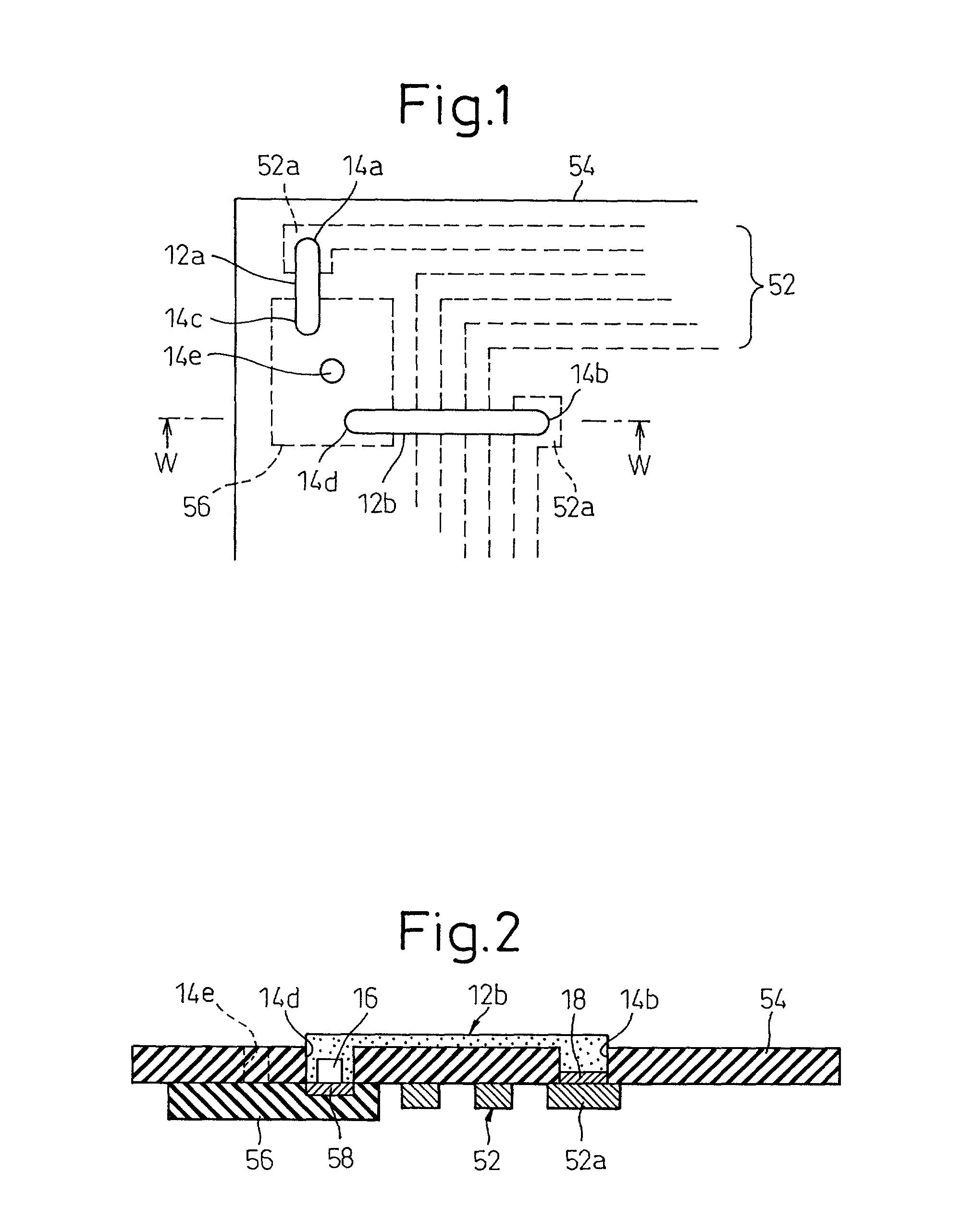
[0037] (First Embodiment)
[0038] A structure of a non-contact type IC card 10 will be described below.
[0039] First of all, among components of the non-contact type IC card, those the same as those in the prior art contact type IC card 50 will be described with reference to FIGS. 6(a) and 6(b).
[0040] A plane coil 52 is formed on a surface of an thin insulating resinous substrate or film 54, and a semiconductor element 56 is mounted on the surface of the thin insulating resinous substrate 54 so that electrode terminals 58 of the former are electrically connected to terminal portions of the plane coil 52, respectively, wherein the semiconductor element 56, the plane coil 51 and the thin insulating resinous substrate 54 are covered with a pair of oversheets 62 applied on the opposite sides of the thin insulating resinous substrate 54 to form an integral piece.
[0041] Next, an electric connection between the plane coil 52 and the semiconductor element 56 will be described, which is one of ...
second embodiment
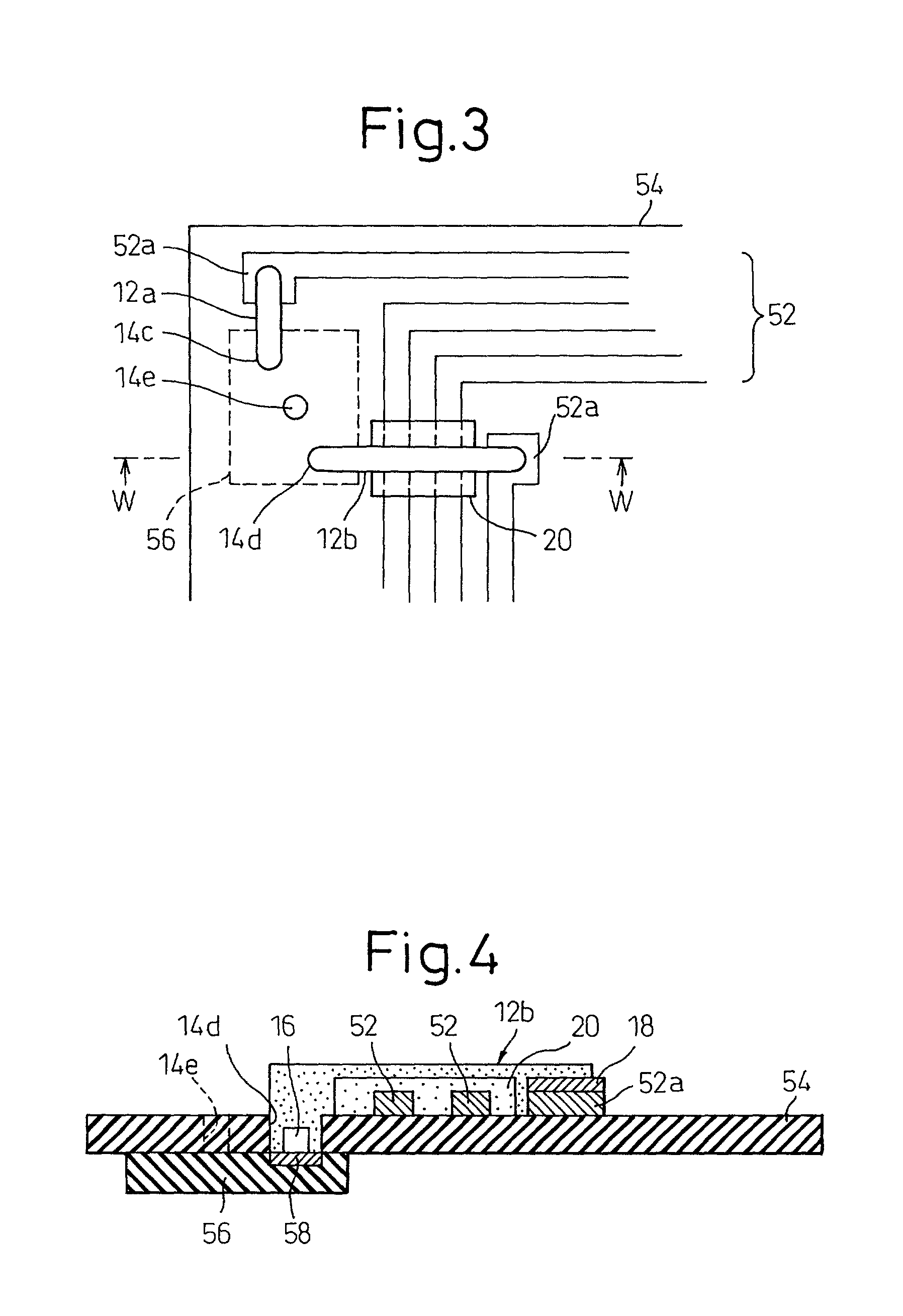
[0057] (Second Embodiment)
[0058] In a second embodiment, the plane coil 52 and the semiconductor element 56 are disposed on different surfaces, respectively, of a thin insulating resinous substrate or film 54 as shown in FIGS. 3 and 4.
[0059] More specifically, the plane coil 52 is disposed on one surface of the thin insulating resinous substrate 54 (the upper surface as seen in FIGS. 3 and 4), whilst the semiconductor element 56 is disposed on the other surface of the thin insulating resinous substrate 54 (the lower surface as seen in FIGS. 3 and 4).
[0060] The connecting structure between the terminal portions 52a of the plane coil 52 and the electrode terminals 58 of the semiconductor element 56 includes the third through-hole 14c and the fourth through-hole 14d provided in the insulating thin resinous substrate 54 for exposing the electrode terminal 58 of the semiconductor element 56 on the one surface, and two circuit patterns 12 (12a, 12b) formed of electro-conductive paste, ext...
PUM
| Property | Measurement | Unit |
|---|---|---|
| Electrical conductor | aaaaa | aaaaa |
| aaaaa | aaaaa |
Abstract
Description
Claims
Application Information
 - R&D Engineer
- R&D Manager
- IP Professional
- Industry Leading Data Capabilities
- Powerful AI technology
- Patent DNA Extraction
Browse by: Latest US Patents, China's latest patents, Technical Efficacy Thesaurus, Application Domain, Technology Topic.
© 2024 PatSnap. All rights reserved.Legal|Privacy policy|Modern Slavery Act Transparency Statement|Sitemap