Minority carrier semiconductor devices with improved reliabilty

Inactive Publication Date: 2002-01-10
LUMILEDS
View PDF0 Cites 0 Cited by
  • Summary
  • Abstract
  • Description
  • Claims
  • Application Information

AI Technical Summary

Benefits of technology

0010] A first preferred embodiment of the present invention comprises a method for improving the operating stability of minority carrier semiconductor devices by the intentional introduction of impurities into the layers adjacent to the active region, which impurities act as a barrier to the degradation process, particularly undesired defect formation and propagation. The semiconductor devices produced using this method also comprise this first embodiment of the i

Problems solved by technology

Normally, O is considered an efficient deep level

Method used


Image

  • Minority carrier semiconductor devices with improved reliabilty
  • Minority carrier semiconductor devices with improved reliabilty
  • Minority carrier semiconductor devices with improved reliabilty

Examples


Embodiment Construction

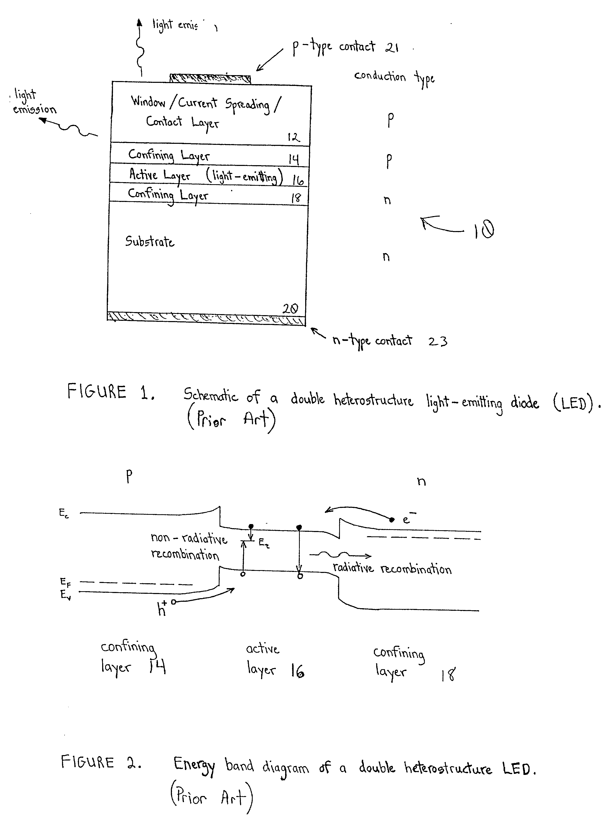
[0012] FIG. 1 is a cross-sectional drawing of a known light emitting semiconductor device;

[0013] FIG. 2 is an energy band diagram of the light emitting semiconductor device shown in FIG. 1;

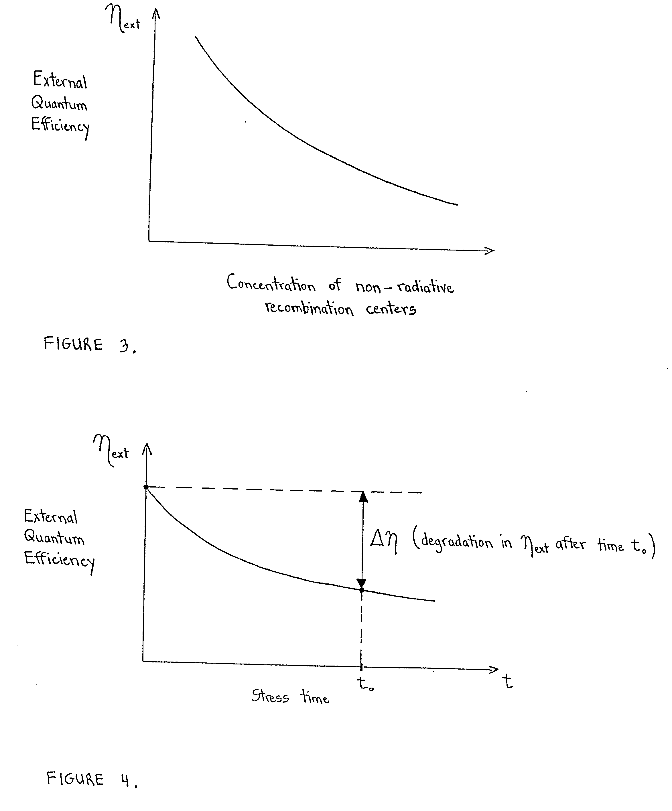
[0014] FIG. 3 is a graph of the concentration of non-radiative recombination centers versus the external quantum efficiency of the device shown in FIG. 1;

[0015] FIG. 4 is a graph of the stress time versus the external quantum efficiency of the device shown in FIG. 1;

[0016] FIG. 5 shows the effect of O in the active layer on .eta..sub.external;

[0017] FIG. 6 shows the effect of O in the p-type confining layer on .DELTA..eta..sub.external;

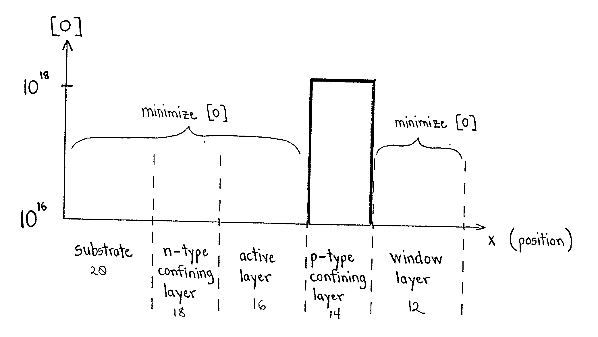
[0018] FIG. 7 is a graph showing the concentration of oxygen in each of the layers of a semiconductor device as taught by the first preferred embodiment of the present invention; and

[0019] FIG. 8 is a graph of the external quantum efficiency .eta..sub.external of devices constructed according to the present invention versus stress time.

[0020] High efficiency visible...


PUM


Abstract

A method for improving the operating stability of compound semiconductor minority carrier devices and the devices created using this method are described. The method describes intentional introduction of impurities into the layers adjacent to the active region, which impurities act as a barrier to the degradation process, particularly undesired defect formation and propagation. A preferred embodiment of the present invention uses O doping of III-V optoelectronic devices during an epitaxial growth process to improve the operating reliability of the devices.

Description

[0001] This invention is in the field of minority carrier semiconductor devices. The invention relates in particular to methods for improving the operating stability of light emitting semiconductor devices by the intentional introduction of impurities and the devices created using these methods.[0002] Degradation of semiconductor minority carrier devices typically involves an increase in the non-radiative recombination efficiency of the device during the device's operation. The causes of this degradation depend on the type of device, its structure, materials, and operating conditions.[0003] A known double heterostructure light emitting diode ("LED") is shown in FIG. 1. LED 10 is comprised of an optically transparent GaP window / current spreading / contact layer 12, high bandgap AlInP upper confining / injection layer 14, a lower bandgap (Al.sub.xGa.sub.1-x).sub.0.-5In.sub.0.5P active layer 16, high bandgap AlInP lower confining / injection layer 18, and conductive substrate 20, which may b...

Claims


Application Information

Patent Timeline
IPC IPC(8): H01L29/207H01L33/30H01S5/30
CPCH01L29/207H01L33/305H01S5/305Y10S257/918
Inventor STOCKMAN, STEPHEN A.STEIGERWALD, DANIEL A.CHEN, CHANGHUA
Owner LUMILEDS
Why Eureka
Try Eureka