
Electroluminescent device with anthracene derivative host

Active Publication Date: 2005-09-29
GLOBAL OLED TECH
View PDF14 Cites 179 Cited by
  • Summary
  • Abstract
  • Description
  • Claims
  • Application Information

AI Technical Summary

Benefits of technology

[0011] Embodiments of the invention provide high luminance yield, have improved operational stability and a desirable hue and that are conveniently manufactured.

Problems solved by technology

While organic electroluminescent (EL) devices have been known for over two decades, their performance limitations have represented a barrier to many desirable applications.
However, anthracenes substituted in such positions may be difficult and expensive to manufacture and may not provide all the desirable embodiments of a host material.

Method used


Image

  • Electroluminescent device with anthracene derivative host
  • Electroluminescent device with anthracene derivative host
  • Electroluminescent device with anthracene derivative host

Examples


example 1

DEVICE EXAMPLE 1

EL Device Fabrication of Samples 1-6

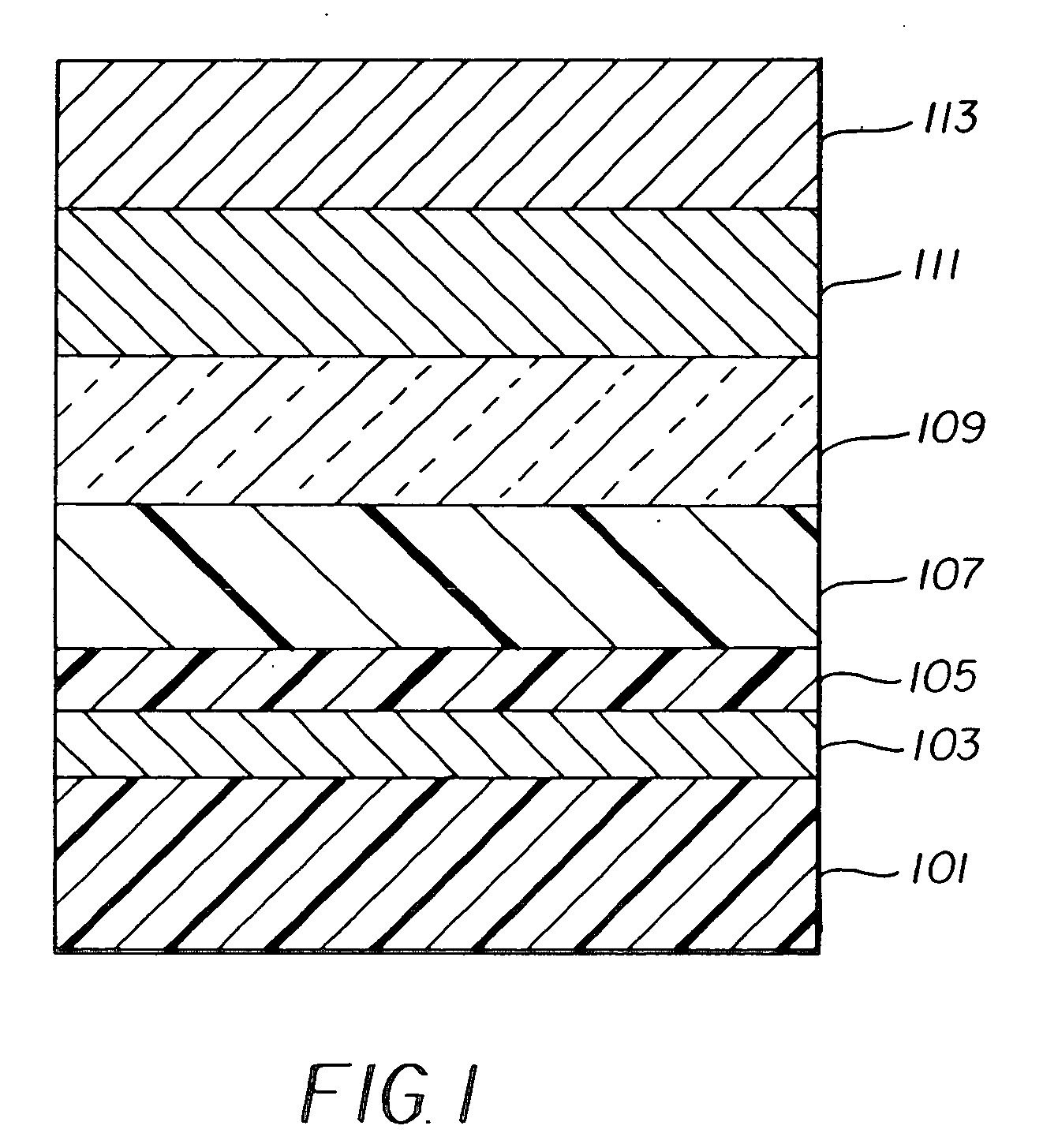
[0158] An EL device (Sample 1) satisfying the requirements of the invention was constructed in the following manner: [0159] 1. A glass substrate coated with an 85 nm layer of indium-tin oxide (ITO) as the anode was sequentially ultrasonicated in a commercial detergent, rinsed in deionized water, degreased in toluene vapor and exposed to oxygen plasma for about 1 min. [0160] 2. Over the ITO was deposited a 1 nm fluorocarbon (CFx) hole-injecting layer (HIL) by plasma-assisted deposition of CHF3. [0161] 3. A hole-transporting layer (HTL) of N,N′-di-1-naphthyl-N,N-diphenyl-4,4′-diaminobiphenyl (NPB) having a thickness of 75 nm was then evaporated from a tantalum boat. [0162] 4. A 20 nm light-emitting layer (LEL), including host material Inv-1 and light-emitting material TBP (2,5,8,11-tetra-t-butylperylene, 1.00 vol %), was then deposited onto the hole-transporting layer. These materials were also evaporated from tantalum boats. [0163]...

example 2

DEVICE EXAMPLE 2

EL Device Fabrication of Samples 7-12

[0169] EL devices, Samples 7-11, were fabricated in an identical manner as Sample 1-5, except Inv-1 was replaced with Inv-2. Sample 12 was prepared in the same manner as Sample 6. The devices thus formed were tested for in the same manner as Samples 1-6, except the devices were tested for stability by operating the cells at 20 mA / cm2 for 200 h at 70° C. The testing results are reported in Table 2.

TABLE 2Evaluation Results for EL devices 7-12.HostTBPLevelLevelYield200 hSampleHost(nm)(vol %)(cd / A)CIExCIEyStabilityType7Inv-22001.003.350.1640.26486%Invention8Inv-24001.003.270.1740.32184%Invention9Inv-22002.002.880.1650.25789%Invention10Inv-24002.003.300.1750.32987%Invention11Inv-22004.001.710.3110.53880%Invention12TBADN2001.502.860.1440.21783%Comparison

[0170] It can be seen from Table 2 that the anthracene material of the invention, Inv-2, affords a good luminance yield and operating stability relative to a comparison anthracene ma...

example 3

DEVICE EXAMPLE 3

EL Device Fabrication of Samples 13-18

[0171] EL devices, Samples 7-11, were fabricated in an identical manner as Sample 1-5, except Inv-1 was replaced with Inv-3. Sample 18 was prepared in the same manner as Sample 6. The devices thus formed were tested for in the same manner as Samples 1-6, except the devices were tested for stability by operating the cells at 20 mA / cm2 for 200 h at 70° C. The testing results are reported in Table 3.

TABLE 3Evaluation Results for EL devices 13-18.HostTBPLevelLevelYield200 hSampleHost(nm)(vol %)(cd / A)CIExCIEyStabilityType13Inv-32001.003.520.1700.28588%Invention14Inv-34001.004.260.1740.32887%Invention15Inv-32002.003.440.1700.28591%Invention16Inv-34002.004.140.1750.33589%Invention17Inv-32004.003.150.1770.30989%Invention18TBADN2001.502.870.1420.20575%Comparison

[0172] It can be seen from Table 3 that the anthracene material of the invention, Inv-3, affords a high luminance yield and very good operating stability relative to a compariso...


PUM

PropertyMeasurementUnit
Lightaaaaaaaaaa

Abstract

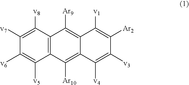
An electroluminescent device comprises a light emitting layer including an anthracene material bearing at least one aryl ring in the 2-position and having a hydrogen or an alkyl group in the 6-position and having up to 12 aromatic carbocyclic rings including at least one naphthalene group in the 9-position of the anthracene group and an aryl group in the 10-position, the anthracene material including among the rings only carbocyclic rings.

Description

FIELD OF INVENTION [0001] This invention relates to organic electroluminescent (EL) devices comprising a light-emitting layer containing a host and a light-emitting material where the host comprises a particular anthracene compound with good operational stability. BACKGROUND OF THE INVENTION [0002] While organic electroluminescent (EL) devices have been known for over two decades, their performance limitations have represented a barrier to many desirable applications. In simplest form, an organic EL device is comprised of an anode for hole injection, a cathode for electron injection, and an organic medium sandwiched between these electrodes to support charge recombination that yields emission of light. These devices are also commonly referred to as organic light-emitting diodes, or OLEDs. Representative of earlier organic EL devices are Gurnee et al. U.S. Pat. No. 3,172,862, issued Mar. 9, 1965; Gurnee U.S. Pat. No. 3,173,050, issued Mar. 9, 1965; Dresner, “Double Injection Electrol...

Claims


Application Information

Patent Timeline
IPC IPC(8): C09K11/06H01L51/00H01L51/30H01L51/50H05B33/14
CPCC09K11/06C09K2211/1011H01L51/0058H05B33/14H01L51/0062H01L51/0081H01L51/5012H01L51/0059H10K85/649H10K85/626H10K85/631H10K85/324H10K50/11
Inventor CONLEY, SCOTT R.VREELAND, WILLIAM B.COSIMBESCU, LELIA
Owner GLOBAL OLED TECH
Learn More