

Method for eliminating standing waves in a photoresist profile
- Summary
- Abstract
- Description
- Claims
- Application Information
AI Technical Summary
Benefits of technology
Problems solved by technology
Method used
Image

Examples
Embodiment Construction
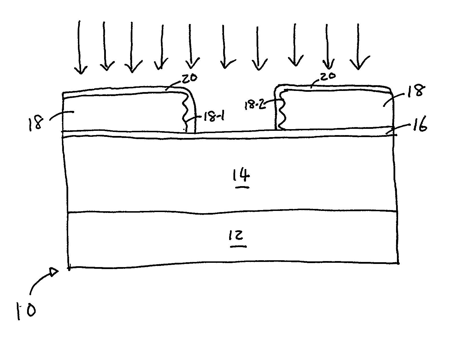
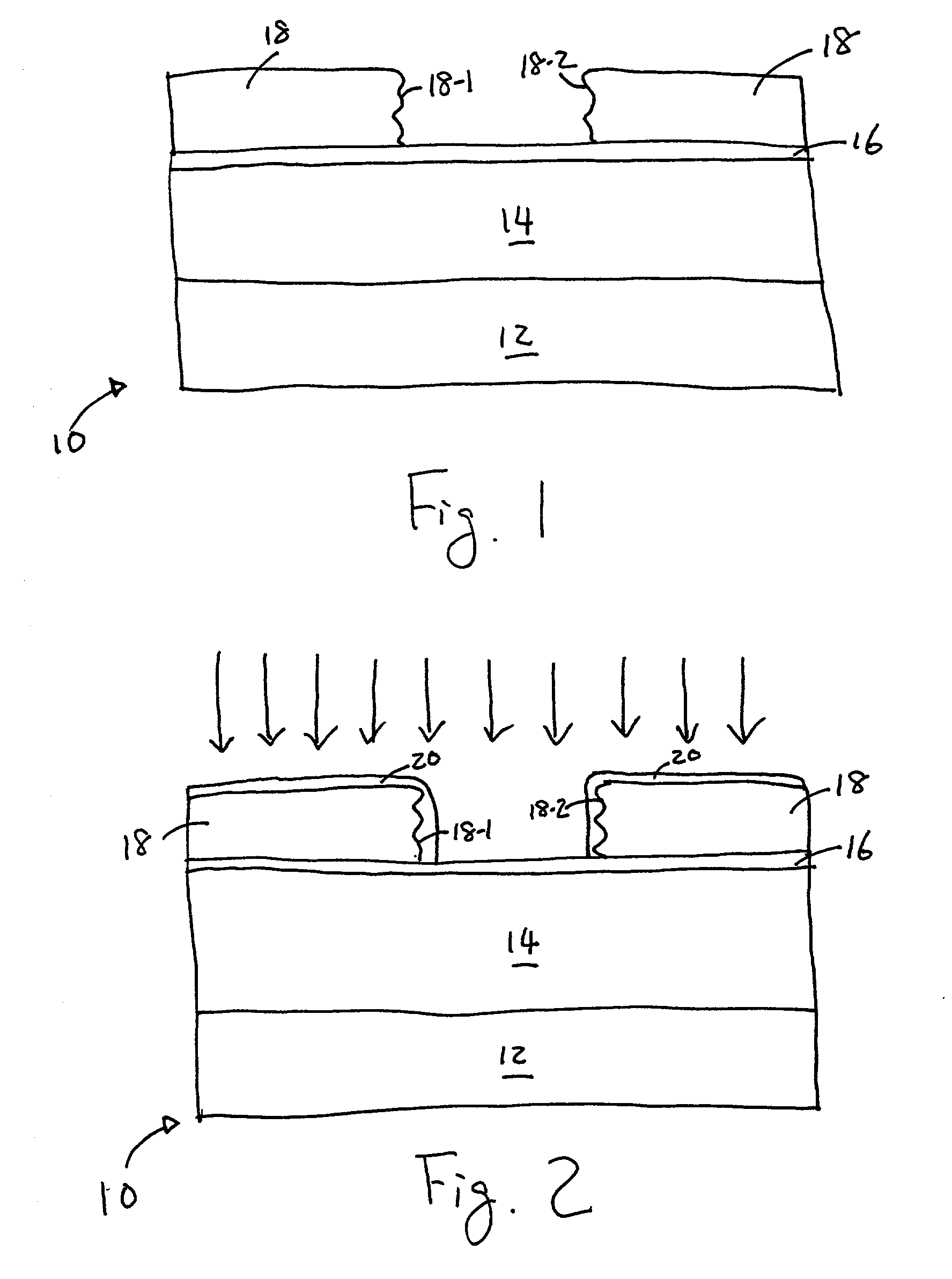
[0001] 1. Field of the Invention
[0002] This invention relates in general to a semiconductor manufacturing process and, more particularly, to a novel manufacturing process to improve conventional photolithographic methods.
[0003] 2. Background of the Invention
[0004] With sub-micron semiconductor manufacturing process being the prevalent technology, the demand for a high-resolution photolithographic process has increased. The resolution of a conventional photolithographic method is primarily dependent upon the wavelength of a light source, which dictates that there be a certain fixed distance between patterns on a photoresist. In addition, conventional photolithographic methods often leave a rough profile on vertical surfaces of an etched photoresist due to the characteristics of conventional etching processes. A photoresist having a rough profile often presents itself in the shape of a "standing wave" on the photoresist surfaces. The lack of uniformity on the photoresist surfaces may ...
PUM
 Abstract
Description
Claims
Application Information