Microsystem packaging and associated methods

a technology of micro-systems and packaging, applied in the direction of instruments, optical elements, and details of semiconductor/solid-state devices, can solve the problems of affecting the performance of the device, causing the device to be damaged, adversely affecting the performance,

Inactive Publication Date: 2004-03-11
CORNING INC
View PDF0 Cites 134 Cited by
  • Summary
  • Abstract
  • Description
  • Claims
  • Application Information

AI Technical Summary

Problems solved by technology

Die bow or warping can occur from thermo-mechanical stresses in the device and packaging, and can damage the device, or adversely influence its performance.
Thermo-mechanical stress in the devices are caused by thermal mismatch, such as coefficient of thermal expansion (CTE) mismatches between the die and packaging materials.
CTE mismatches result in movement of materials relative to each other from temperature changes, resulting in stress in the materials.
However, conventional hermetic packaging using CTE matching materials has been found to be both expensive, and not particularly effective at reducing die warpage.
This is largely due to the limited choice of materials available for conventional hermetic packaging.
These available materials generally do not have very closely matching CTEs and / or are expensive.
Furthermore, for microsystem devices using magnets, it is generally difficult to include the magnets in conventional hermetically sealed packaging.
Also, magnets often require active alignment of their magnetic fields with respect to active structures, which is difficult to achieve inside of a hermetically sealed package.

Method used


Image

  • Microsystem packaging and associated methods
  • Microsystem packaging and associated methods
  • Microsystem packaging and associated methods

Examples


Embodiment Construction

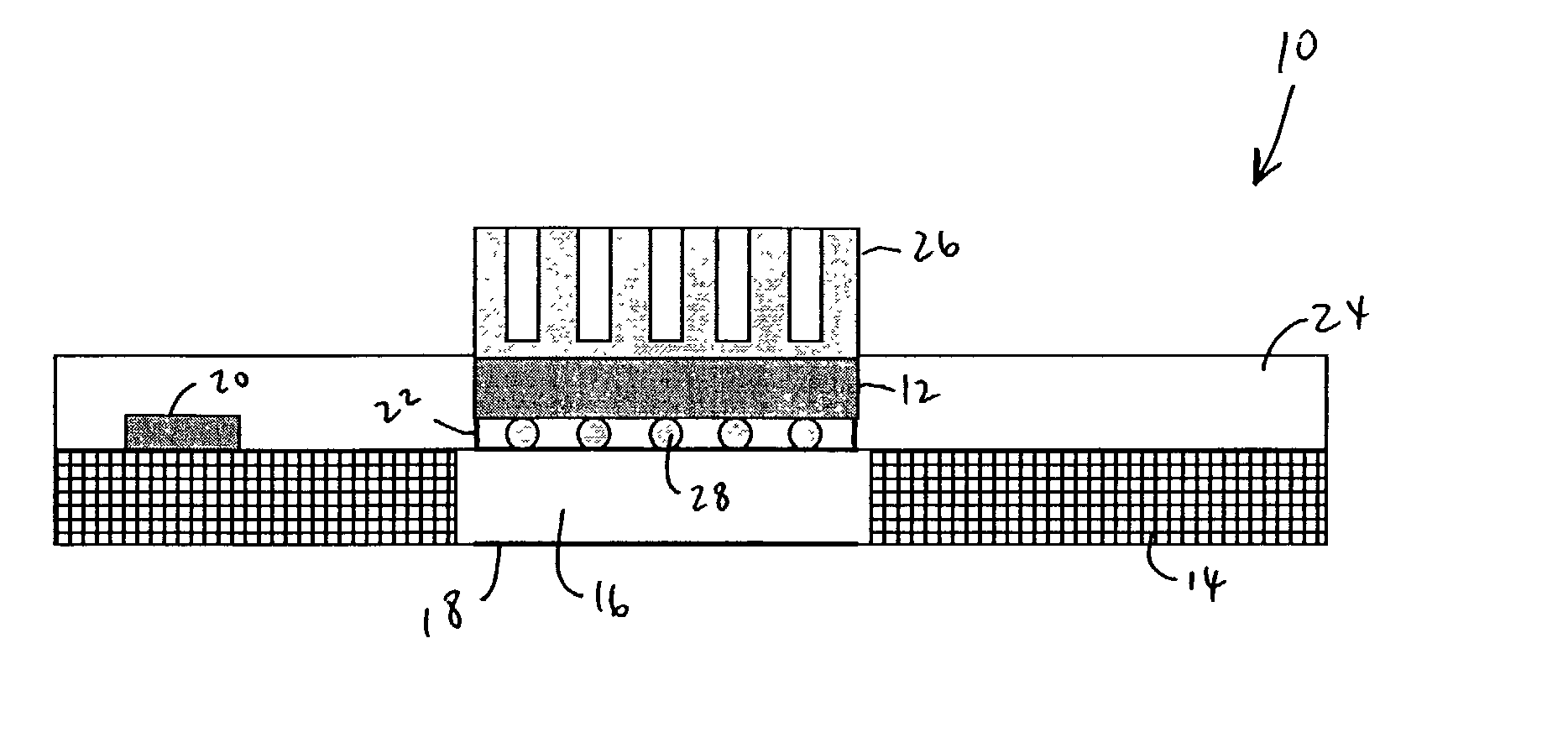
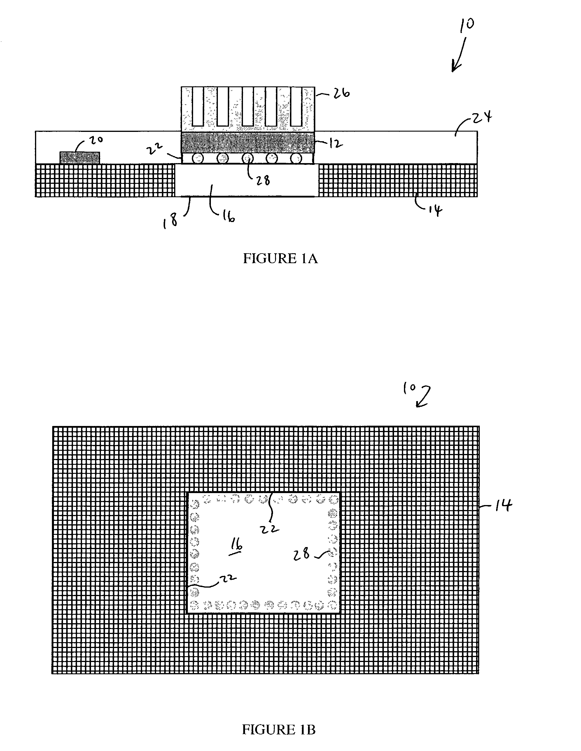
[0008] In accordance with some embodiments of the invention, a microsystem package is provided including a microsystem device having a device die, and a substrate to which the microsystem device is flip chip bonded. The substrate has a CTE substantially matching that of the device die, and includes an opening for transmission of signals therethrough to the device.

[0009] In accordance with some embodiments of the invention, a microsystem package is provided including a microsystem device and a substrate having a recess for receiving the microsystem device. A material is provided between sides of the microsystem device and sidewalls defining the recess in the substrate for reducing thermo-mechanical stresses applied to the microsystem device.

[0010] In accordance with some embodiments of the invention, a microsystem device package is provided including a substrate having an opening extending therethrough, a microsystem device flip chip bonded to one side of the substrate around the ope...


PUM


Abstract

Methods and apparatus are provided for sealing and reducing warpage in a microsystem device. The microsystem device is assembled with a substrate and packaged.

Description

[0001] 1. Field of the Invention[0002] The present invention relates generally to microsystem devices and, more particularly, to methods and apparatus for packaging microsystem devices and maintaining the flatness of such devices, and to the integration of magnet assemblies into microsystem packages, and methods for hermetically sealing such packages.[0003] 2. Description of Related Art[0004] Microsystem devices include, but are not limited to, optical microelectromechanical system (MOEMS) devices, microelectromechanical system (MEMS) devices, electro-optical devices, electromechanical devices, electrothermal devices, piezoelectric devices, electromagnetic devices, electrostatic devices, and any combination of such devices with one another or with electronic devices. These devices generally include a die or chip on which the functional components of the device are fabricated. For example, in a magnetic MEMS mirror device, the functional components can include selectively rotatable m...

Claims


Application Information

Patent Timeline
Patent Type & Authority Applications(United States)
IPC IPC(8): B81B7/00G02B6/42H01L21/58H01L23/13H01L23/14H01L23/16H01L23/31
CPCB81B7/0048G02B6/4232H01L23/13H01L23/14H01L23/16H01L23/3121H01L24/73H01L24/83H01L2224/131H01L2224/32014H01L2224/48091H01L2224/48227H01L2224/73204H01L2224/83194H01L2224/8385H01L2924/01013H01L2924/01018H01L2924/01027H01L2924/01049H01L2924/01078H01L2924/01079H01L2924/01082H01L2924/01322H01L2924/07802H01L2924/09701H01L2924/12044H01L2924/15153H01L2924/15165H01L2924/1532H01L2924/3511H01L24/32H01L24/48H01L2224/2919H01L2924/00013H01L2924/01006H01L2924/01033H01L2924/014H01L2924/0665H01L2224/29109H01L2224/29111H01L2924/0132H01L2924/0133H01L2224/16225H01L2224/73257H01L2224/13109H01L2224/13111H01L2924/1815H01L2924/15311H01L2924/00014H01L2224/13099H01L2924/00H01L2924/01026H01L2924/01028H01L2924/01029H01L2924/01047H01L2924/0105H01L2924/01083H01L2224/05599H01L2224/45099H01L2224/85399H01L2924/12042H01L2924/15787H01L2924/181H01L2224/45015H01L2924/207
Inventor WAELTI, MARCBOWMAN, AMY CATHERINETAYLOR, WILLIAM PATRICKZOU, JIN
Owner CORNING INC
Why Eureka
Try Eureka