Semiconductor device having a Cu interconnection and method for manufacturing the same

a technology of semiconductor devices and interconnections, which is applied in the direction of semiconductor devices, semiconductor/solid-state device details, electrical devices, etc., can solve the problem of not providing a sufficient amount of metallic atoms

Inactive Publication Date: 2004-08-05
NEC ELECTRONICS CORP
View PDF6 Cites 26 Cited by
  • Summary
  • Abstract
  • Description
  • Claims
  • Application Information

AI Technical Summary

Problems solved by technology

The technique using a seed film for diffusing metallic atoms therefrom does not provid...

Method used


Image

  • Semiconductor device having a Cu interconnection and method for manufacturing the same
  • Semiconductor device having a Cu interconnection and method for manufacturing the same
  • Semiconductor device having a Cu interconnection and method for manufacturing the same

Examples


first embodiment

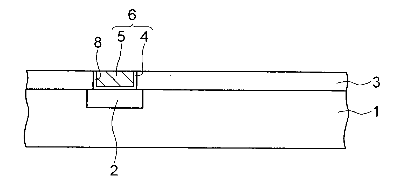
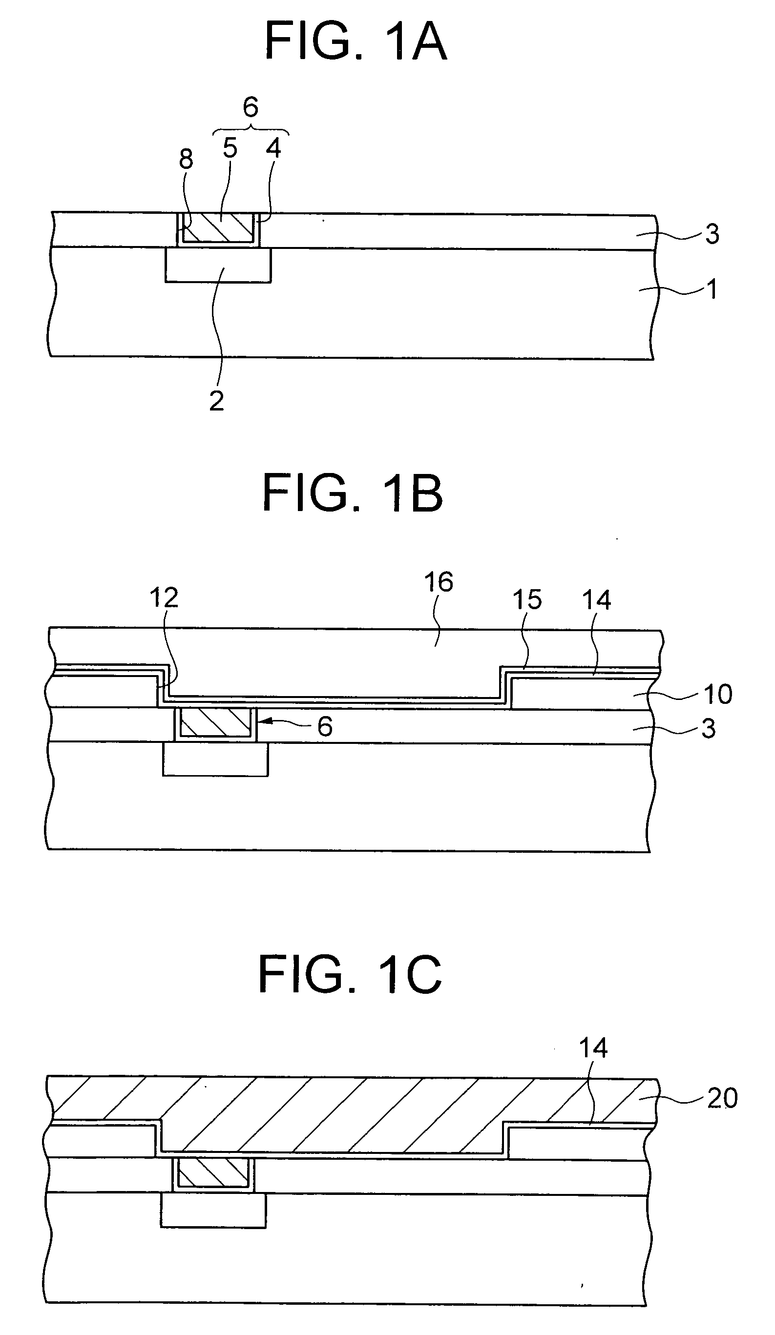
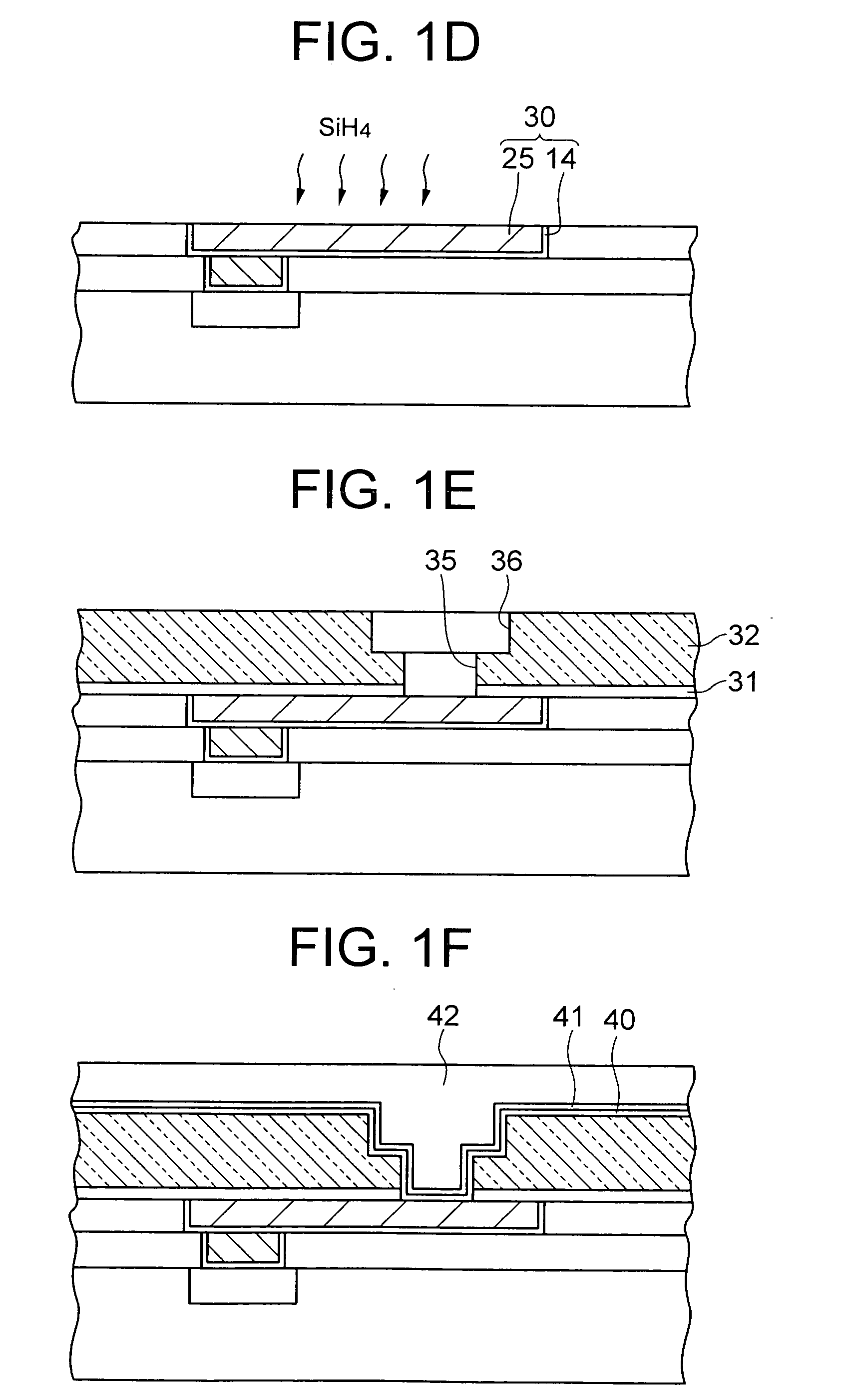
[0020] FIGS. 1A to 1I show a fabrication process for manufacturing a semiconductor device according to the present invention. In FIG. 1A, a dielectric film 3 is formed on the surface of a silicon substrate 1 including therein diffused regions 2 of semiconductor elements such as transistors. The dielectric film 3 has therein a contact hole 8, which exposes therefrom the diffused region 2 on the silicon substrate 1. The contact hole 8 receives therein an embedded conductor 6. The embedded conductor 6 includes a barrier metal film 4 and a tungsten plug 5, the barrier metal film 4 having a two-layer structure including a Ti layer (not shown) on the diffused region 2 and an overlying TiN layer (not shown).

[0021] As shown in FIG. 1B, an interlayer dielectric film 10 is deposited on the dielectric film 3 and the embedded conductor 6, followed by formation of an interconnection trench 12 in the interlayer dielectric film 10. The interconnection trench 12 exposes therefrom the embedded condu...

second embodiment

[0038] FIGS. 2A to 21 show a fabrication process for manufacturing a semiconductor device according to the present invention. The present embodiment is applied to a so-called single damascene structure.

[0039] As depicted in FIGS. 2A to 2D, a conductor 6 and a first-layer Cu interconnection 30 are formed on a silicon substrate 1. The first-layer Cu interconnection 30 is connected to the conductor 6, which is in contact with the diffused region 2 formed in the silicon substrate 1.

[0040] Subsequently, as shown in FIG. 2E, a Cu-diffusion suppression film 31 and an interlayer dielectric film 70 are consecutively formed on the entire surface, followed by forming a via hole 71 used in the single damascene structure by selectively etching the Cu-diffusion suppression film 31 and the interlayer dielectric film 70. A barrier metal film 72 including Ta / TaN layers is then formed on the entire surface including the via hole 71, followed by forming consecutively a seed film (not shown) and a Cu f...


PUM


Abstract

A Cu interconnection in a semiconductor device has an ununiform profile of additive metal atoms wherein the additive metal atoms are rich in the vicinities of bottom and side surfaces of the Cu interconnection. The Cu interconnection also has an ununiform silicon profile wherein additive silicon atoms are rich in the vicinity of the top surface of the Cu interconnection. The structure improves the electro-migration resistance and the stress-migration resistance of the Cu interconnection.

Description

[0001] (a) Field of the Invention[0002] The present invention relates to a semiconductor device having a Cu interconnection and a method for manufacturing the same.[0003] (b) Description of the Related Art[0004] Along with development of finer structure and higher integration density of semiconductor elements in a semiconductor device, it has become important to reduce the interconnect resistance in the semiconductor device. As one of the means to reduce the interconnect resistance, a semiconductor device having embedded Cu interconnections is introduced into practical use, wherein Cu is used as the material for the interconnections and a so-called damascene process is used for fabricating the interconnections.[0005] It is to be noted that the interconnections should have a higher electro-migration resistance as well as the reduction of the interconnect resistance as described above. This also applies to the case of embedded Cu interconnections.[0006] To achieve a higher electro-mig...

Claims


Application Information

Patent Timeline
IPC IPC(8): H01L21/3205H01L21/768H01L23/52H01L23/532
CPCH01L21/76807H01L21/76826H01L21/76829H01L21/76834H01L2924/3011H01L21/76883H01L21/76886H01L23/53233H01L21/76877H01L2924/0002H01L2924/00
Inventor TONEGAWA, TAKASHI
Owner NEC ELECTRONICS CORP
Why Eureka
Try Eureka