Modulation circuit including a feedback loop with an embedded mapper

Inactive Publication Date: 2005-02-24
AVAGO TECH INT SALES PTE LTD
View PDF10 Cites 6 Cited by
  • Summary
  • Abstract
  • Description
  • Claims
  • Application Information

AI Technical Summary

Benefits of technology

[0010] In an improved high-fidelity digital modulator, a mapping function is performed within a main feedback loop of the modulator, rather than after the feedback loop. Pulse width modulation mapping in such circuits generates a fairly large harmonic content when cascaded with the digital modulator circuit and tends to dramatically change the shape of the noise floor in the desired band, e.g. 0-40 kHz. In contrast, the inventor has found that placing

Problems solved by technology

However, this dithering function introduces a small but measurable amount of noise into the circuit and therefore reduces signal-to-noise ratios.
Known DACs

Method used


Image

  • Modulation circuit including a feedback loop with an embedded mapper
  • Modulation circuit including a feedback loop with an embedded mapper
  • Modulation circuit including a feedback loop with an embedded mapper

Examples


Embodiment Construction

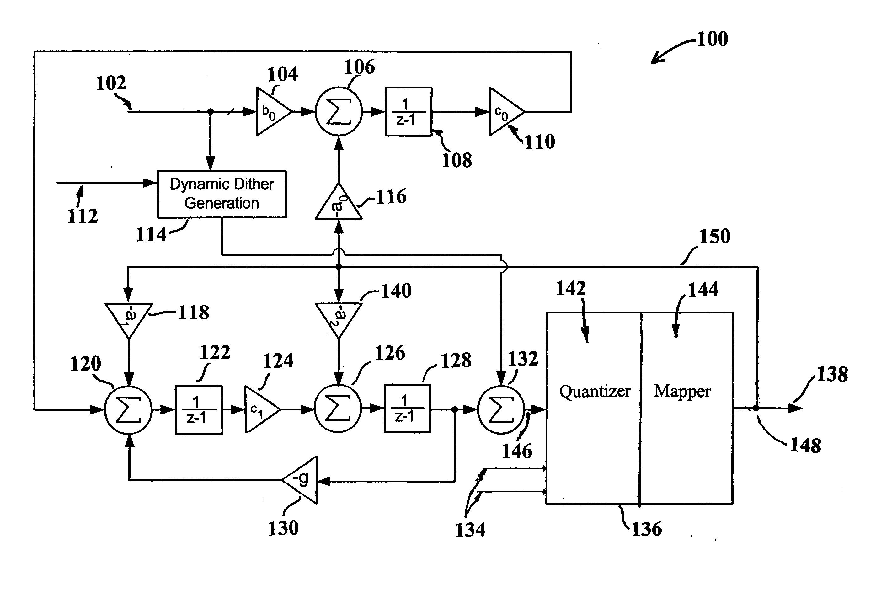
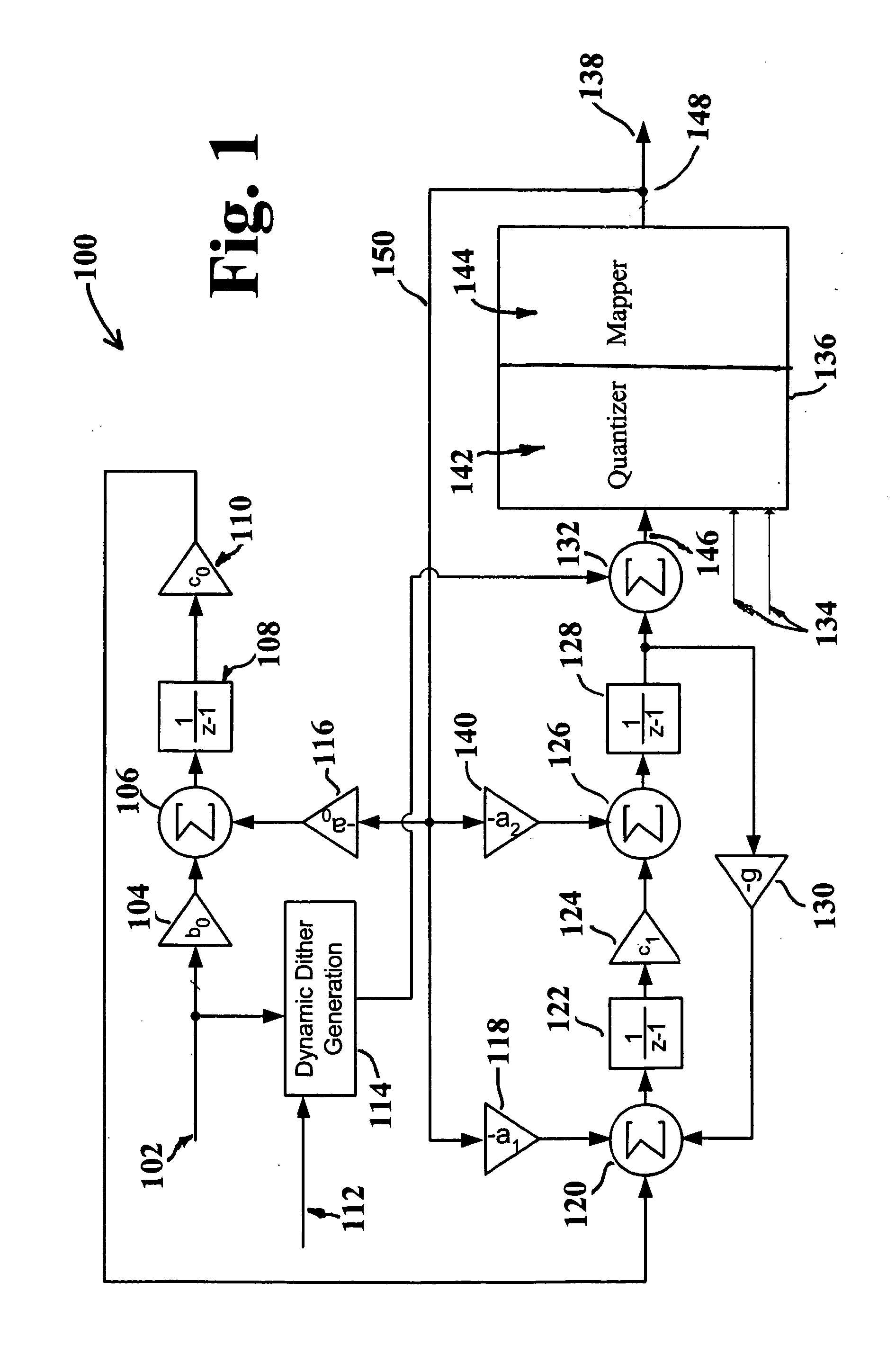
[0019] The invention will be described with reference to several exemplary embodiments. FIG. 1 shows a first embodiment of the invention in the form of a digital modulator. In this embodiment, a pulse width modulation mapping function is performed within a high-gain digital modulator feedback loop, rather than subsequent to the feedback loop. In FIG. 1, the digital modulator is shown generally at 100. Digital modulator 100 has an input 102 and an output 138. The circuit of digital modulator 100 comprises a gain stage 104, a summing point 106, an integrator 108, a gain stage 110, a dither control input 112, a dither generation circuit 114, a gain stage 116, a gain stage 118, a summing point 120, an integrator 122, a gain stage 124, a summing point 126, an integrator 128, a gain stage 130, a summing point 132, one or more clock inputs 134, a gain stage 140, and a mapping circuit 136 incorporating a quantizer 142 and a mapper 144. Mapping circuit 136 has an input 146 and a feedback poi...


PUM


Abstract

In a modulator circuit, a mapping function is performed within a main feedback loop of the modulator, rather than after the feedback loop. In a high-fidelity digital modulator embodiment, pulse width modulation mapping generates a fairly large harmonic content when cascaded with the digital modulator circuit and tends to dramatically change the shape of the noise floor in the desired band, e.g. 0-40 kHz. Placing the mapping function within the modulator feedback loop tends to compensate for non-linear features of the mapping function, thus reducing harmonic generation and simplifying the task of suppressing harmonic generation to an acceptable level. In addition to reducing harmonic generation, this arrangement simplifies feedback processing and the accumulation of feedback information within various integrators in the modulator circuit.

Description

[0001] This application is a continuation-in-part of U.S. patent application Ser. No. 10 / 642,736, titled “System and Method for Shaping Dither Signals,” filed Aug. 19, 2003, the entire disclosure of which is incorporated herein by reference.BACKGROUND OF THE INVENTION [0002] 1. Field of the Invention [0003] The present invention relates generally to improved apparatus and methods for mapping pulse widths in digital modulation circuits, and includes particular applications of these circuits to digital modulators of a type useful in high fidelity audio processing. [0004] 2. Related Art [0005] Digital-to-analog converters (DACs) are used to process digital audio signals. Typically digital data signals are received from a digital replay device or over a network, such as a cable television network. The signals are then processed by a DAC in an audio amplifier, cable receiver, or other audio device to produce an analog output within a frequency range that, when connected to a transducer s...

Claims


Application Information

Patent Timeline
IPC IPC(8): H03M3/00
CPCH03M3/332H03M3/334H03M3/454H03M3/448H03M3/412H03M3/3287
Inventor MILLER, KEVIN LEE
Owner AVAGO TECH INT SALES PTE LTD
Why Eureka
Try Eureka