Castellated chip-scale packages and methods for fabricating the same

a chip-scale package and chip-scale technology, applied in the direction of semiconductor devices, semiconductor/solid-state device details, electrical apparatus, etc., can solve the problems of undesirably large amount of real estate on the carrier substrate, undesirably large distance between semiconductor device packages, and undesirably high profile of the assembly

Active Publication Date: 2005-03-31
MICRON TECH INC
View PDF55 Cites 117 Cited by
  • Summary
  • Abstract
  • Description
  • Claims
  • Application Information

AI Technical Summary

Benefits of technology

[0018] As an example, a wafer or other large-scale substrate carrying a plurality of semiconductor devices, which is referred to herein as a “semiconductor substrate,” may be secured to a sacrificial, or “dummy,” substrate. The sacrificial substrate may include lower contact pad sections, which are referred to herein as “lower sections” for simplicity, or precursors thereto, which are referred to herein as “precursor pads.” These lower sections or precursor pads are positioned so as to align with corresponding semiconductor devices when the semiconductor substrate is secured to the sacrificial substrate.
[0019] Insulative and redistribution layers are formed over the semiconductor devices by use of known processes. The results are circuit traces that communicate with bond pads and extend from the bond pads toward or to the outer periphery of the semiconductor device. If the contact pads of the chip-scale package under fabrication are to include upper sections, which are positioned adjacent to the active surface of the semiconductor device, the upper sections may also be formed during the fabrication of the redistribution layer, with at least some of the circuit traces extending to corresponding upper sections. The insulative and redistribution layers may be formed either before or after the semiconductor substrate is secured to the sacrificial substrate.
[0020] Once the insulative and redistribution layers have been formed and the semiconductor substrate has been secured to the sacrificial substrate, the semiconductor devices are at least partially severed from one another. If the sacrificial substrate includes lower sections of contact pads, such severing may expose portions (e.g., edges or a surface) of the lower sections. If the sacrificial substrate includes precursor pads thereon, such severing may sever the precursor pads or expose a surface thereof.
[0021] Next, the exposed, outer peripheral edges of the semiconductor devices are coated with an electrically insulative material. Such coating may be followed by a second cut. The result is a peripheral dielectric coating on each peripheral edge of each semiconductor device. At this point in the packaging process, the semiconductor devices that are carried by the semiconductor substrate are substantially separated from one another and are held in place relative to one another by way of the sacrificial substrate. In addition, the outer edges of any lower sections of contact pads are exposed.

Problems solved by technology

Leads typically contribute to the dimensions of the footprint of a conventional semiconductor device package and, thus, consume an undesirably large amount of real estate upon a carrier substrate (e.g., a circuit board) to which the semiconductor device package is to be secured and electrically connected.
When coupled with the thicknesses that conventional encapsulants and carriers impart to the overall thickness of a conventional semiconductor device package, the added heights of such discrete conductive structures may result in a semiconductor device package which will protrude an undesirably large distance from a carrier substrate to which it is secured and electrically connected.
Such spacing of a semiconductor device apart from a carrier substrate may therefore impart the assembly with an undesirably high profile.
Moreover, these types of chip-scale packaging technologies typically do not permit the placement of a chip-scale package on a carrier substrate in a face-up orientation.

Method used


Image

  • Castellated chip-scale packages and methods for fabricating the same
  • Castellated chip-scale packages and methods for fabricating the same
  • Castellated chip-scale packages and methods for fabricating the same

Examples


Embodiment Construction

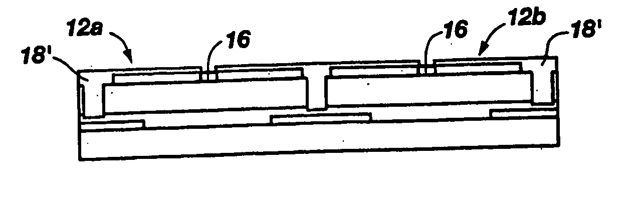
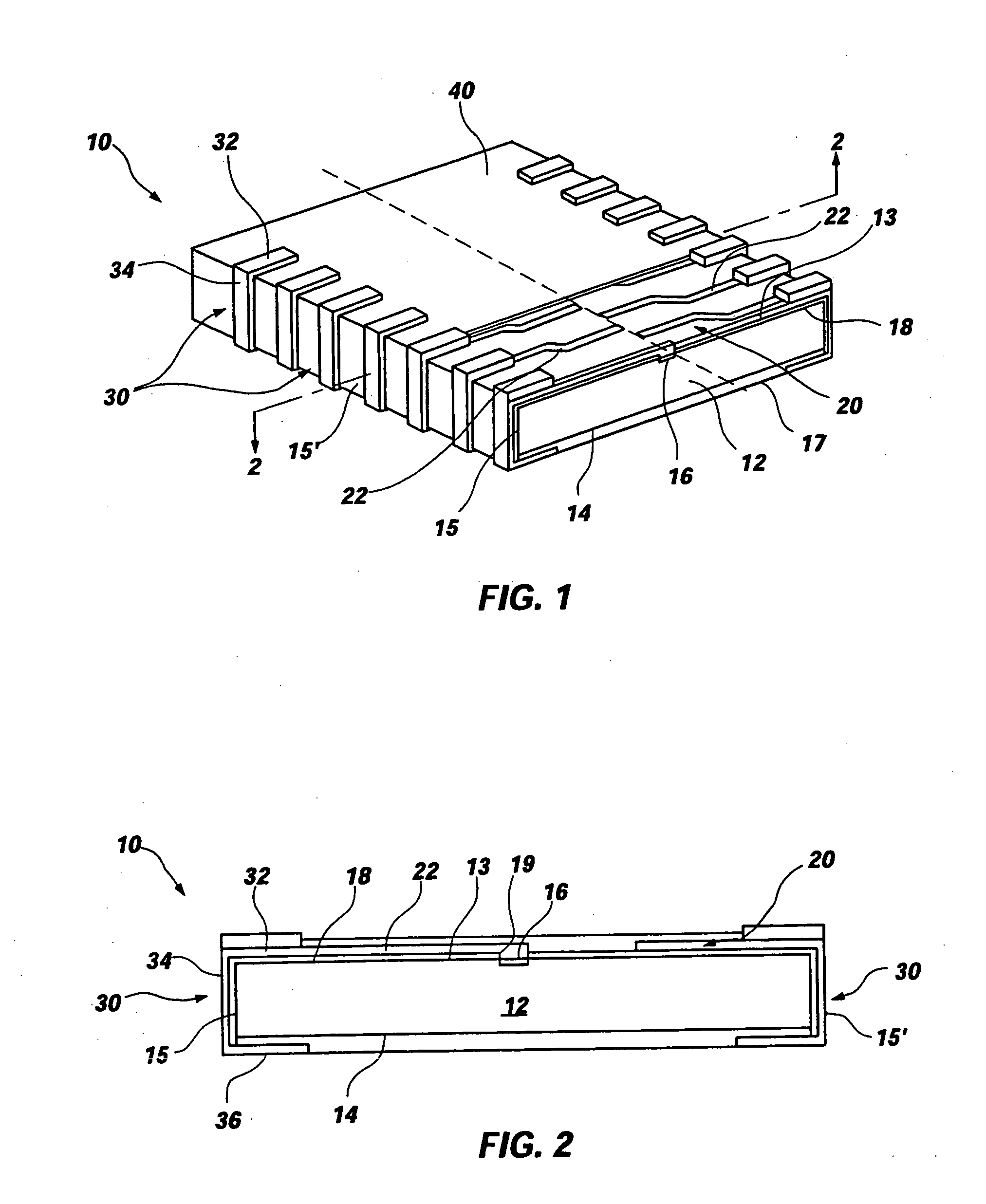
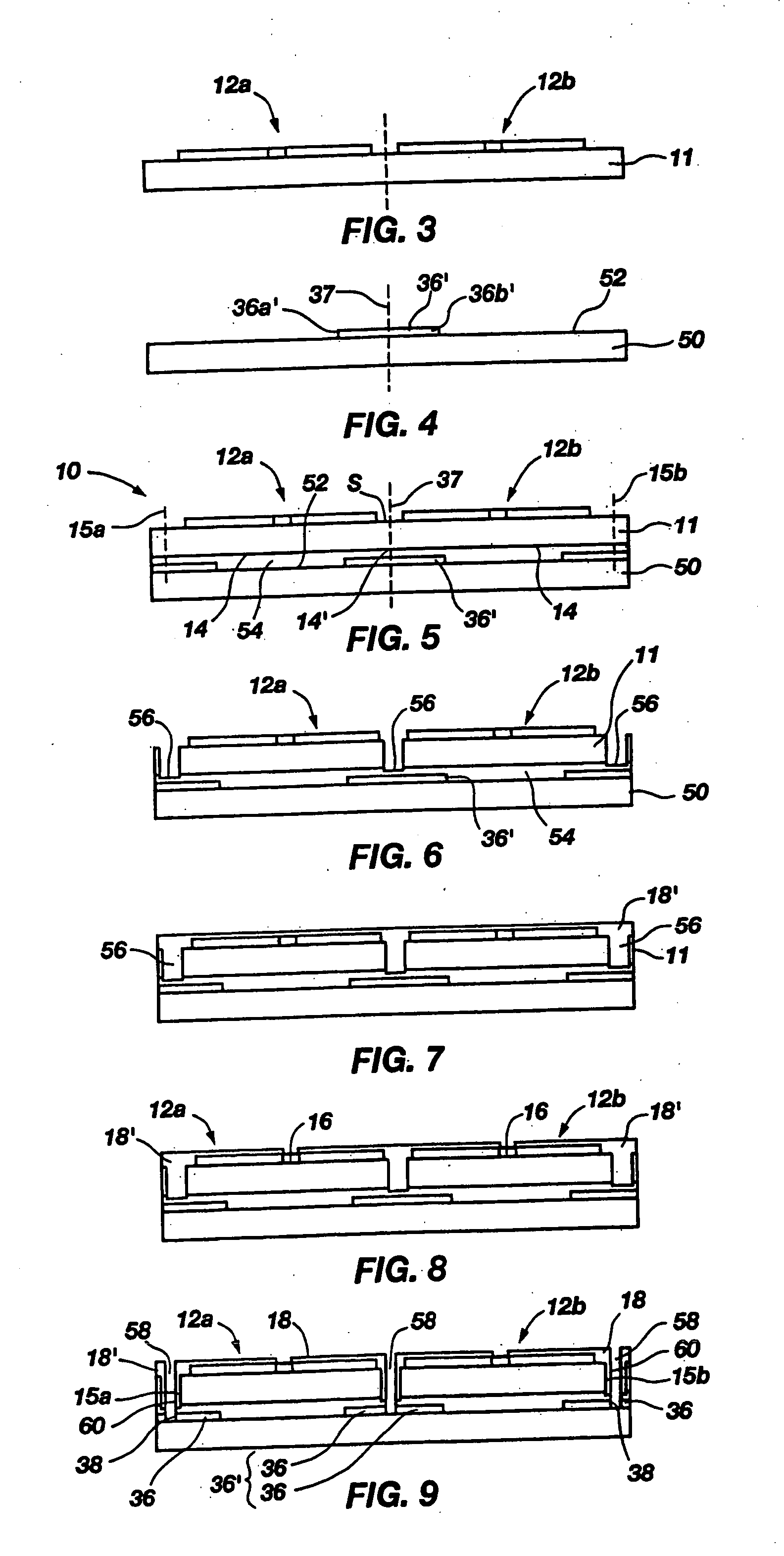
[0041] With reference to FIGS. 1 and 2, an exemplary embodiment of a chip-scale package 10 that incorporates teachings of the present invention is depicted. Chip-scale package 10 includes a semiconductor device 12, a redistribution layer 20 over an active surface 13 thereof, and contact pads 30 that extend from redistribution layer 20, around an outer peripheral edge 15 (also referred to herein as “outer periphery 15”) of semiconductor device 12, and onto a back side 14 of semiconductor device 12. Accordingly, each contact pad 30 includes an upper section 32, a peripheral section 34, and a lower section 36 (see FIG. 2). As contact pads 30 are located adjacent to an outer peripheral edge 15 of semiconductor device 12 and, thus, at an outer peripheral edge 15′ of chip-scale package 10, they impart chip-scale package 10 with a somewhat castellated appearance and, thus, are also referred to herein as “castellated contacts.”

[0042] Semiconductor device 12 includes bond pads 16 on active s...


PUM


Abstract

A method for fabricating a chip-scale package includes securing a device substrate that carries at least two adjacent semiconductor devices to a sacrificial substrate. The sacrificial substrate may include conductive elements on a surface thereof, which are located so as to align along a street between each adjacent pair of semiconductor devices on the device substrate. The device substrate is then severed along each street and the newly formed peripheral edge of each semiconductor device coated with dielectric material. If the sacrificial substrate includes conductive elements, they may be exposed between adjacent semiconductor devices and subsequently serve as lower sections of contacts. Peripheral sections of contacts are formed on the peripheral edge. Upper sections of the contacts may also be formed over the active surfaces of the semiconductor devices. Once the contacts are formed, the sacrificial substrate is substantially removed from the back sides of the semiconductor devices.

Description

BACKGROUND OF THE INVENTION [0001] 1. Field of the Invention [0002] The present invention relates generally to chip-scale packages and, more specifically, to chip-scale packages which include contact pads on both major surfaces thereof, as well as to methods for forming the chip-scale packages. In particular, the present invention relates to chip-scale packages that include castellated contact pads, which include surfaces, or sections, that are exposed at the outer peripheries of such packages, as well as sections that are exposed at both major surfaces of the packages. [0003] 2. Background of Related Art [0004] Conventional semiconductor device packages are typically multi-layered structures. A conventional semiconductor device package may include, for example, a bottom layer of encapsulant material, a carrier, a semiconductor die, and a top layer of encapsulant material. In addition to being located above and beneath the semiconductor die and carrier, the encapsulant material of a...

Claims


Application Information

Patent Timeline
Patent Type & Authority Applications(United States)
IPC IPC(8): H01L21/48H01L21/68H01L23/31H01L23/498H01L25/10
CPCH01L21/4846H01L2225/1058H01L21/6835H01L23/3114H01L23/3121H01L23/49805H01L23/49816H01L24/97H01L25/105H01L2924/01049H01L2924/01075H01L2924/01078H01L2924/09701H01L2924/3025H01L2924/01033H01L2924/12041H01L21/568H01L2924/351H01L2924/12042H01L2924/00
Inventor BOON, SUAN JEUNGCHIA, YONG POOENG, MEOW KOONLOW, SIU WAF
Owner MICRON TECH INC
Why Eureka
Try Eureka