Continuous manufacture of flat panel light emitting devices

a technology of light-emitting devices and manufacturing lines, which is applied in the manufacture of electric discharge tubes/lamps, applications of luminescent coatings, instruments, etc., can solve the problems of difficult deposition of organic materials in the oled device layer, complication of holding and transporting individual discrete substrates, and inconvenient continuous manufacturing techniques

Active Publication Date: 2005-05-19
GLOBAL OLED TECH
View PDF9 Cites 31 Cited by
  • Summary
  • Abstract
  • Description
  • Claims
  • Application Information

AI Technical Summary

Problems solved by technology

The deposition of the layers of organic materials in an OLED device is difficult.
However, this technique is not convenient for continuous manufacture.
A problem with this approach is the complication of holding and transporting individual discrete substrates.
A problem with this approach is the difficulty in making, handling, and cleaning a continuous mask through which multiple depositions are to be made, and the difficulty in maintaining alignment with a continuous substrate and continuous mask for multiple depositions.
In addition, continuous masks are expensive to manufacture.

Method used


Image

  • Continuous manufacture of flat panel light emitting devices
  • Continuous manufacture of flat panel light emitting devices
  • Continuous manufacture of flat panel light emitting devices

Examples


Embodiment Construction

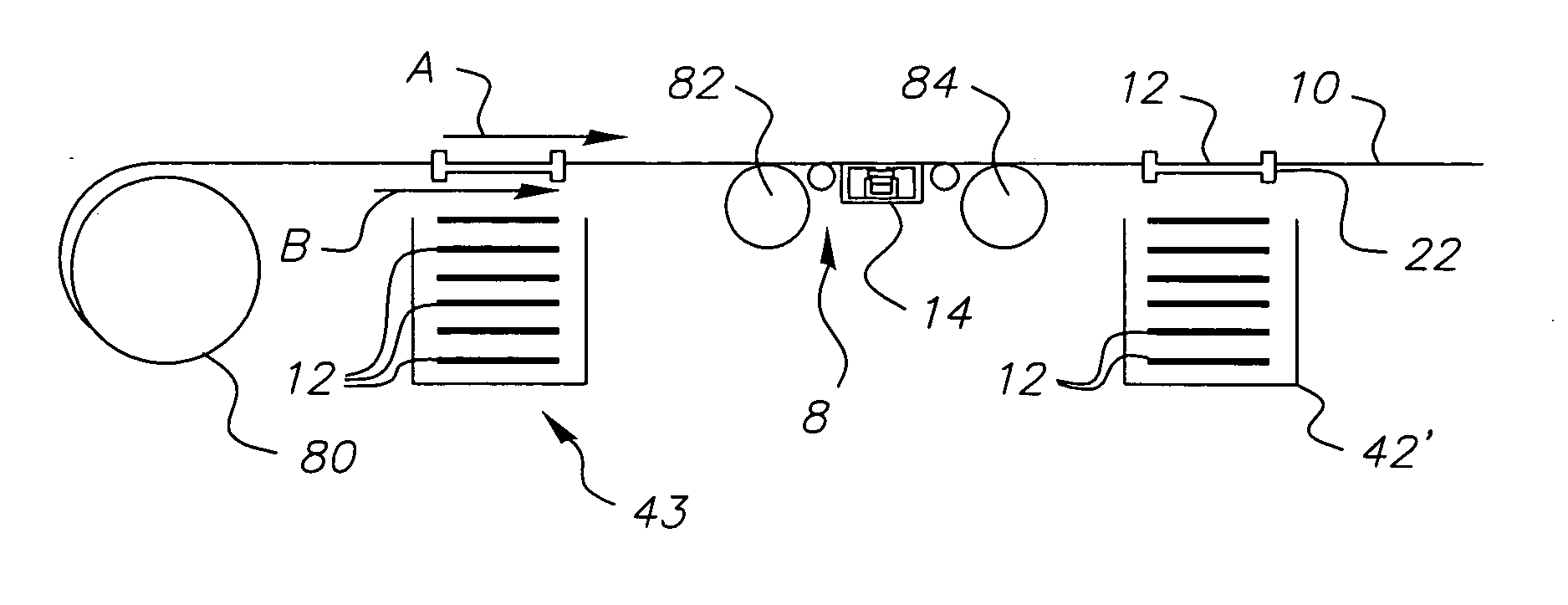
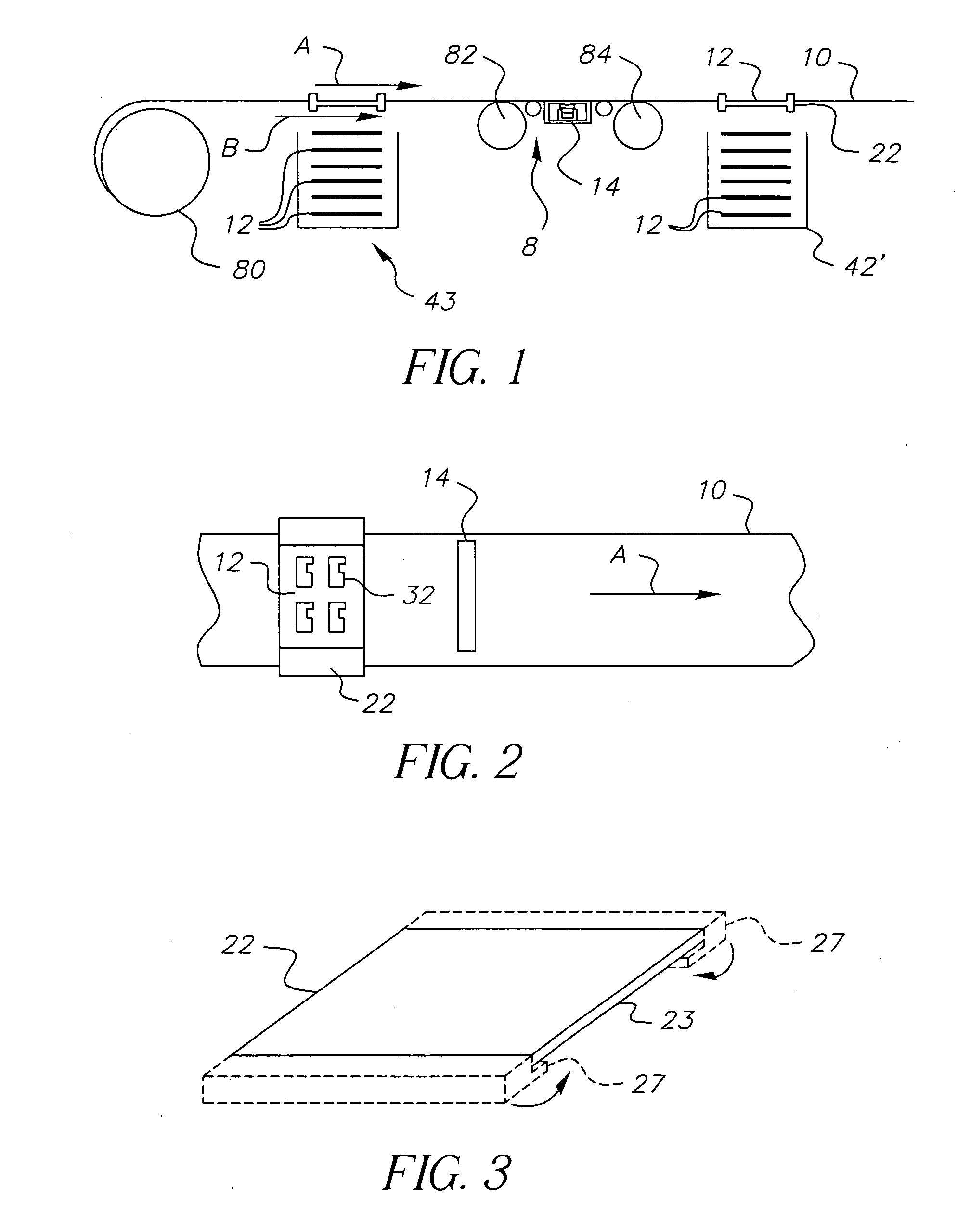
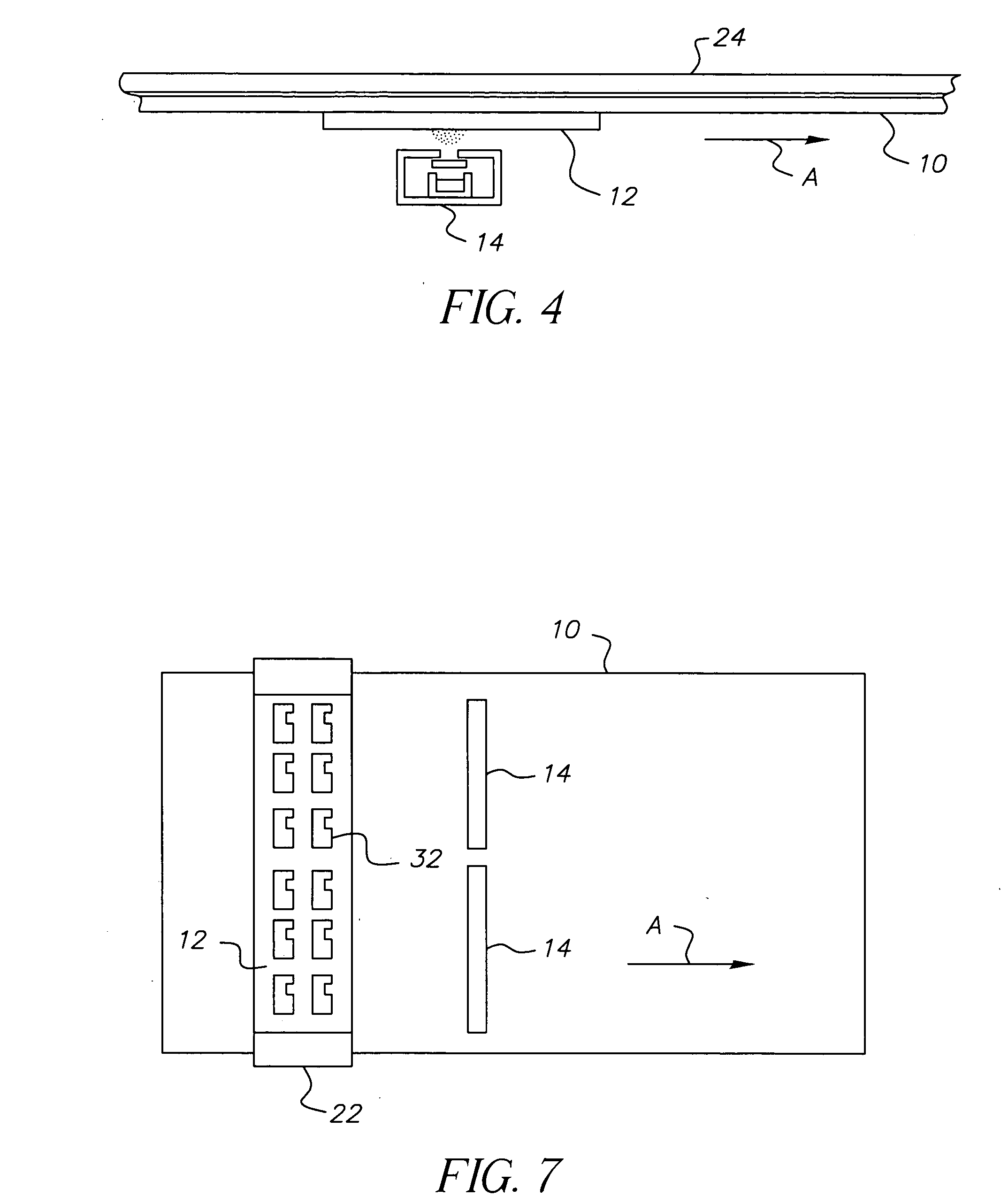
[0019] Referring to FIGS. 1 and 2, a method of applying patterned materials for manufacture of a flat panel display, includes providing a continuous flexible display substrate 10, supplied for example on a roll 80; providing one or more application stations 8, the application stations 8 having one or more stationary sources 14 of material, a supply of patterned masks 12 for defining a pattern of material to be applied to the display substrate 10, means such as clamps 22 for attaching the discrete patterned masks to the substrate and means (such as powered rollers 82, 84) for transporting the display substrate 10 and the patterned masks 12 in registration past the one or more stationary sources 14 of material, and means 43 for delivering the masks one at a time to the transporting means and transporting the display substrate 10 past the one or more application stations 8. The direction of movement of the substrate 10 and mask 12 are shown by arrows A and B in FIG. 1 and in subsequent...


PUM

PropertyMeasurementUnit
flexibleaaaaaaaaaa
magneticaaaaaaaaaa
mechanicalaaaaaaaaaa

Abstract

A method of applying patterned materials for manufacture of a flat panel light source includes providing a flexible continuous substrate; providing one or more application stations, each application station having, one or more stationary sources of material, a supply of discrete patterned masks for defining a pattern of material to be applied to the substrate, means for attaching the discrete patterned masks to the substrate; means for transporting the substrate and the patterned mask in registration past the one or more stationary sources of material, and means for delivering the masks one at a time to the transporting means; and transporting the substrate and the masks past the one or more application stations.

Description

FIELD OF THE INVENTION [0001] The present invention relates to the manufacture of flat panel light emitting devices such as displays and extended light sources, an example being organic light emitting diode displays, backlights and area illumination sources and, more particularly, to the patterned deposition of materials such as organic light emitting materials on a substrate. BACKGROUND OF THE INVENTION [0002] Organic light emitting diode (OLED) light sources and displays are known. Such light sources and displays are constructed by depositing and treating multiple layers of materials such as organic materials on a substrate. When a current is passed through the multiple layers of organic materials, light is emitted. The color of light is dependent on the type of materials. As used herein the term flat panel light source refers to displays, backlights, and area illumination devices. [0003] The deposition of the layers of organic materials in an OLED device is difficult. The materia...

Claims


Application Information

Patent Timeline
Patent Type & Authority Applications(United States)
IPC IPC(8): C23C14/04C23C14/56G02F1/1333H01L27/15H01L27/32H01L51/00H01L51/40H01L51/56H05B33/10
CPCC23C14/042C23C14/562H01L27/15H01L27/32H01L2251/5338H01L51/0002H01L51/0097H01L51/56H01L51/0001H10K59/00H10K71/10H10K71/00H10K77/111H10K2102/311
Inventor COK, RONALD S.STRIP, DAVID R.COURNOYER, ROBERT F.
Owner GLOBAL OLED TECH
Why Eureka
Try Eureka