Coupler assembly for an optical backplane system

Inactive Publication Date: 2005-06-23
RPX CORP +1
View PDF7 Cites 22 Cited by
  • Summary
  • Abstract
  • Description
  • Claims
  • Application Information

AI Technical Summary

Benefits of technology

[0006] Problems in the prior art are addressed, in accordance with the principles of the present invention, by a coupler assembly adapted to optically couple a circuit pack to a backplane in an optical backplane system, which can accommodate possible misalignment between the circuit pack and the backplane and is adapted to correct (1) initial misalignment typically present when the circuit pack is first connected to the backplane and (2) without further intervention from an operator, subsequent misalignment typically caused by mechanical vibrations and/or temperature-induced deformations. To this end, the coupler assembly may employ a movable optical element that can automatically track changes in the relative position of the backplane and the circuit pack to maintain good optical coupling. In one embodime

Problems solved by technology

As complexity of telecommunications and computer systems increases, signals within backplanes are driven at increased clock speeds.
However, at relatively high clock speeds (e.g., over 1 GHz), the performance of electrical buses may become unsatisfactory due to dispersi

Method used


Image

  • Coupler assembly for an optical backplane system
  • Coupler assembly for an optical backplane system
  • Coupler assembly for an optical backplane system

Examples


Embodiment Construction

[0011] Reference herein to “one embodiment” or “an embodiment” means that a particular feature, structure, or characteristic described in connection with the embodiment can be included in at least one embodiment of the invention. The appearances of the phrase “in one embodiment” in various places in the specification are not necessarily all referring to the same embodiment, nor are separate or alternative embodiments mutually exclusive of other embodiments.

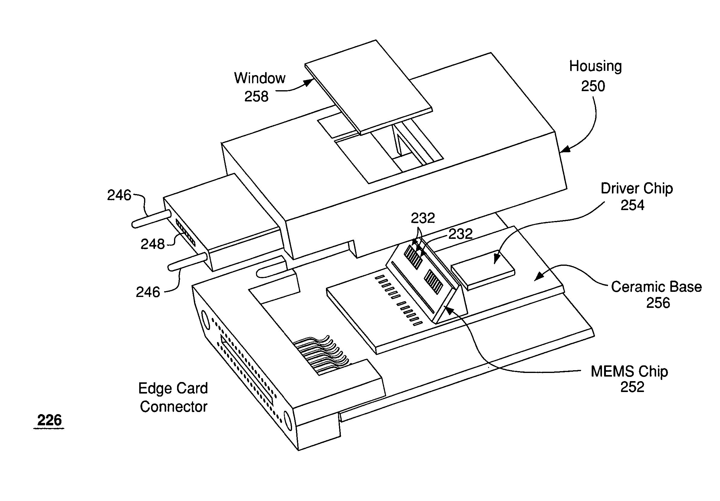
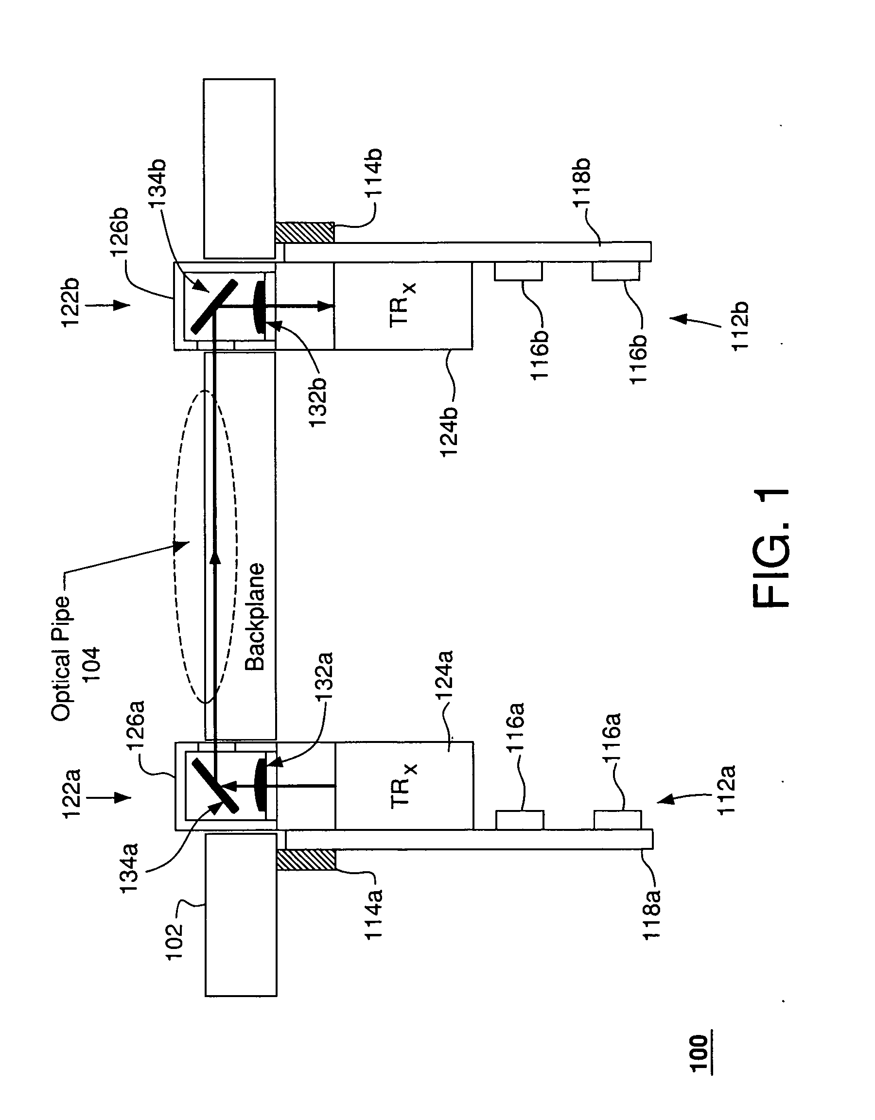
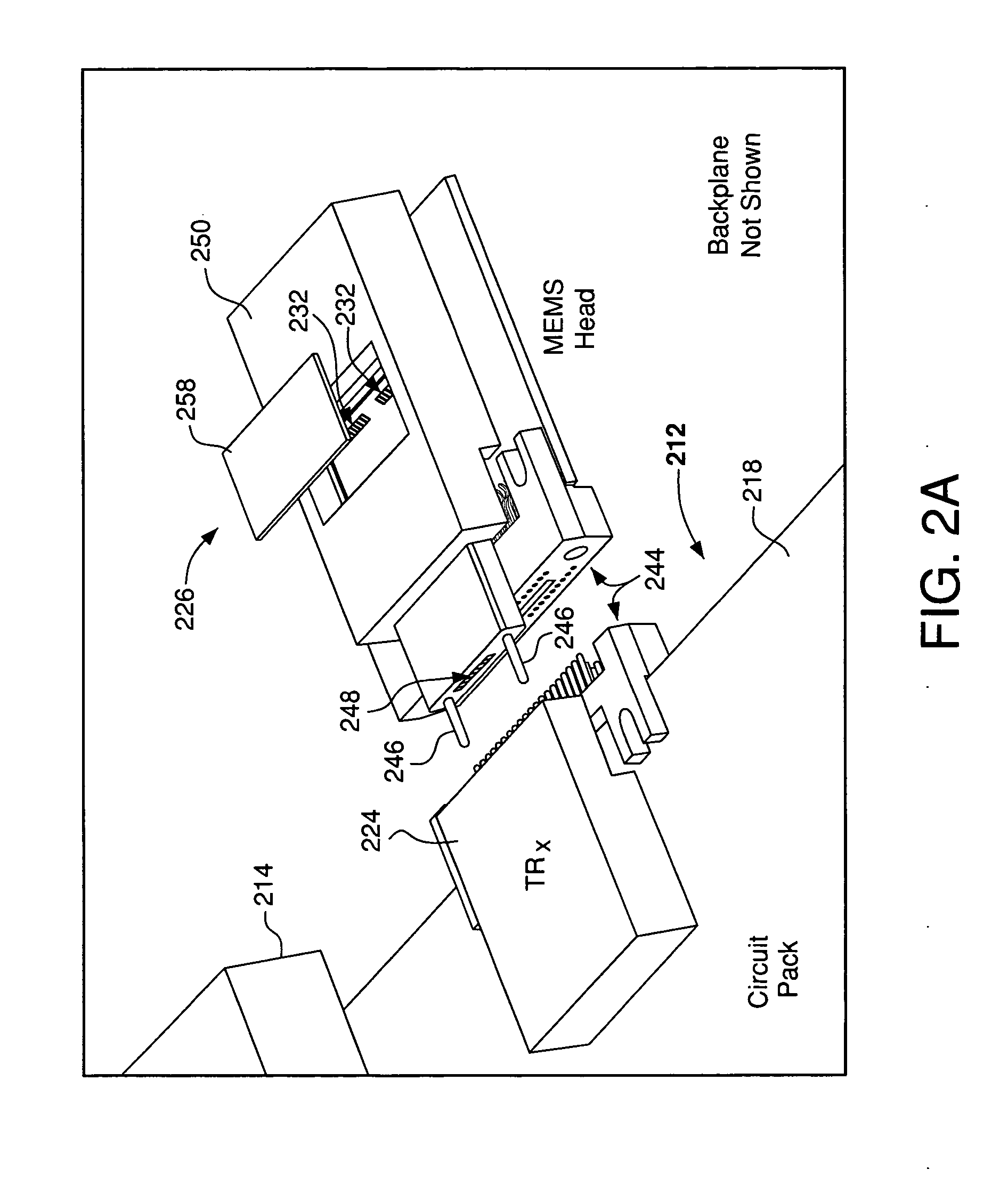
[0012]FIG. 1 shows a cross-sectional view of a backplane / circuit-pack assembly 100 according to one embodiment of the present invention. Assembly 100 has a backplane 102 having an optical pipe 104 adapted to transmit optical signals through the backplane. In one embodiment, backplane 102 is a printed circuit board having an integrated array of optical waveguides that forms optical pipe 104 similar to the optical waveguides described in an article by E. Griese, “A High-Performance Hybrid Electrical-Optical Interconnection Technolo...


PUM


Abstract

A coupler assembly for an optical backplane system having a backplane and two or more circuit packs connected to that backplane. Each circuit pack has an optical transceiver and the backplane has an optical pipe (e.g., an array of waveguides) adapted to guide optical signals between the transceivers of different circuit packs. A coupler assembly is provided for each transceiver to couple light between that transceiver and the optical pipe. Advantageously, the coupler assembly has a movable optical element that can accommodate possible misalignment between the backplane and the circuit pack. In one embodiment, the movable optical element is an array of MEMS mirrors, each mirror adapted to direct light between an optical transmitter or receiver and the corresponding waveguide of the optical pipe. In another embodiment, the movable optical element is an array of flexible optical fibers, each coupled between an optical transmitter or receiver and the corresponding waveguide of the optical pipe and having an angled surface adapted to couple light between said fiber and waveguide.

Description

BACKGROUND OF THE INVENTION [0001] 1. Field of the Invention [0002] The present invention relates to optical circuits and, more specifically, to printed circuit board assemblies having optical circuit components. [0003] 2. Description of the Related Art [0004] A modern telecommunications or computer system typically has a number of printed circuit boards (PCBs) or cards, which plug into a backplane or motherboard. The backplane generally provides power to the PCBs and a pathway by which the PCBs communicate with each other. For most backplanes, an electrical bus, which is typically a series of wires, is a primary means by which the communication between the PCBs takes place. Electrical transmission characteristics of the bus are defined by its material properties, the physical layout of the components, the clock speed of the signals, etc. As complexity of telecommunications and computer systems increases, signals within backplanes are driven at increased clock speeds. However, at re...

Claims


Application Information

Patent Timeline
IPC IPC(8): G02B6/36G02B6/35G02B6/38G02B6/42G02B6/43
CPCG02B6/3502G02B6/3512G02B6/43G02B6/3897G02B6/4292G02B6/3598G02B6/36
Inventor BASAVANHALLY, NAGESH R.RAMSEY, DAVID A.TANG, HONG
Owner RPX CORP
Why Eureka
Try Eureka