Optical connector assembly, coupling device and method for aligning such a coupling device and a waveguide structure
A technology of optical connectors and coupling devices, which is applied to the coupling of optical waveguides, light guides, optical components, etc., and can solve problems such as inability to ensure simultaneous alignment
- Summary
- Abstract
- Description
- Claims
- Application Information
AI Technical Summary
Problems solved by technology
Method used
Image
Examples
Embodiment Construction
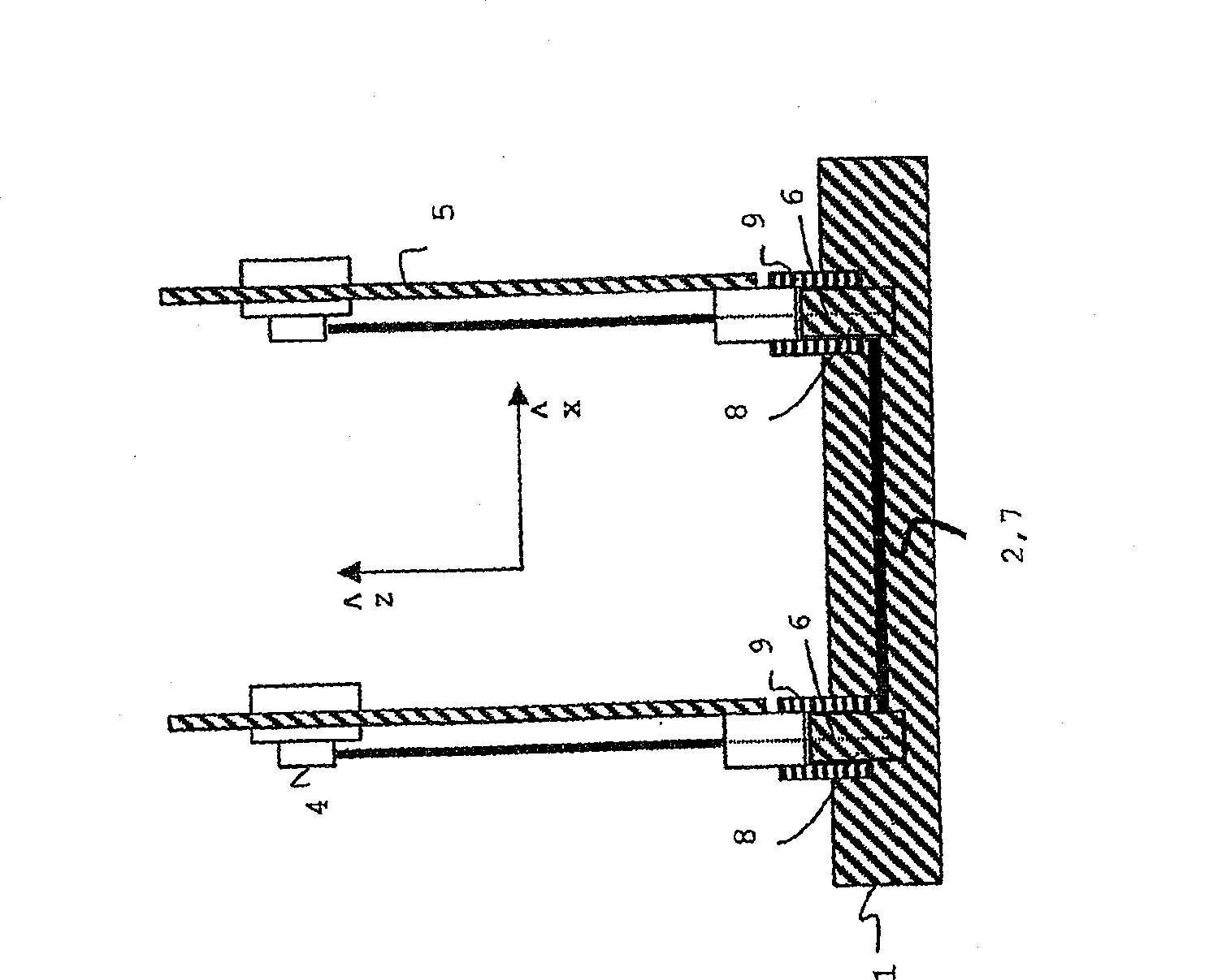
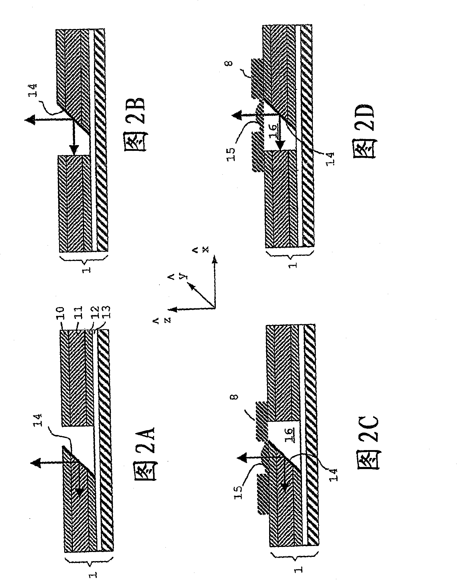
[0028] figure 1 Indicates the mixed light backplane or PCB 1, which is a stack consisting of several layers. Hereinafter, this base plate 1 is also referred to as laminate 1 . Laminate 1 comprises at least: an optical waveguide 2, and it can be the partial waveguide structure 3 that comprises a plurality of waveguides 2 (see Figure 3A ). Waveguide 2 is placed perpendicular to figure 1 in the x-y plane of the midplane. The waveguide 2 or waveguide structure 3 is integrated or embedded in at least one layer of the stack 1 . The embedded waveguide 2 can be a polymer waveguide, a glass sheet waveguide or a waveguide made by embedded optical fiber technology.
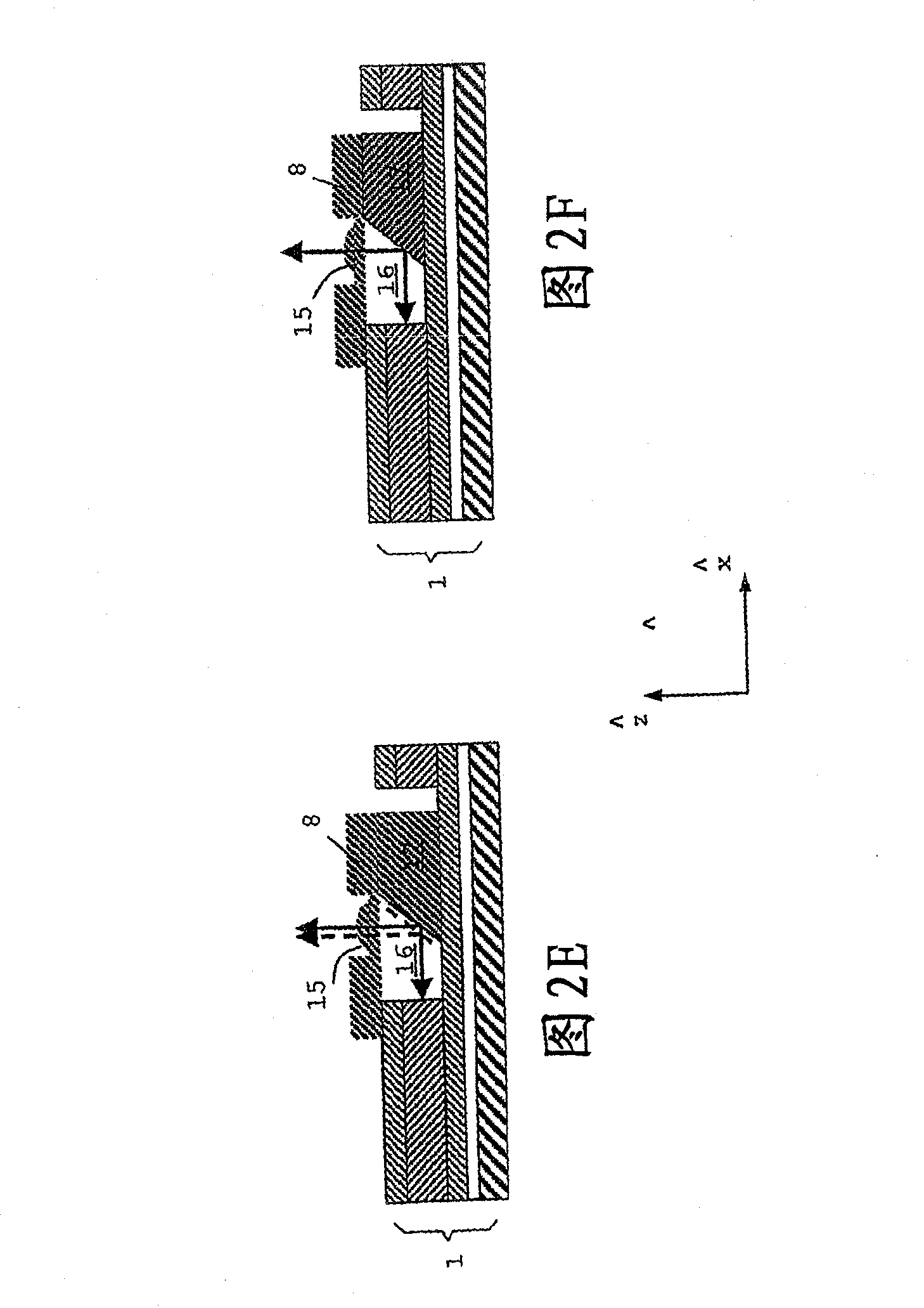
[0029] The optical signal is transferred to or from a cooperating optical device, e.g. an optical or optoelectronic device 4 or another PCB 5, which is on a first optical path 6 of a waveguide 2 in the stack 1, which provides a second optical path for the optical signal Process 7. In order to achieve optimum optical ...
PUM
 Abstract
Description
Claims
Application Information


