
Method of and apparatus for performing sequential processes requiring different amounts of time in the manufacturing of semiconductor devices
a technology of sequential process and semiconductor device, which is applied in the direction of lighting and heating apparatus, charge manipulation, furnaces, etc., can solve the problems of undesired native oxide growing on the surface of the wafer, affecting the production efficiency of the respective unit process, and affecting the production efficiency of the respective unit. achieve the effect of high production efficiency, high efficiency and no significant downtim
- Summary
- Abstract
- Description
- Claims
- Application Information
AI Technical Summary
Benefits of technology
Problems solved by technology
Method used
Image

Examples
Embodiment Construction
[0027] The preferred embodiments of the present invention will hereinafter be described in detail with reference to accompanying drawings.
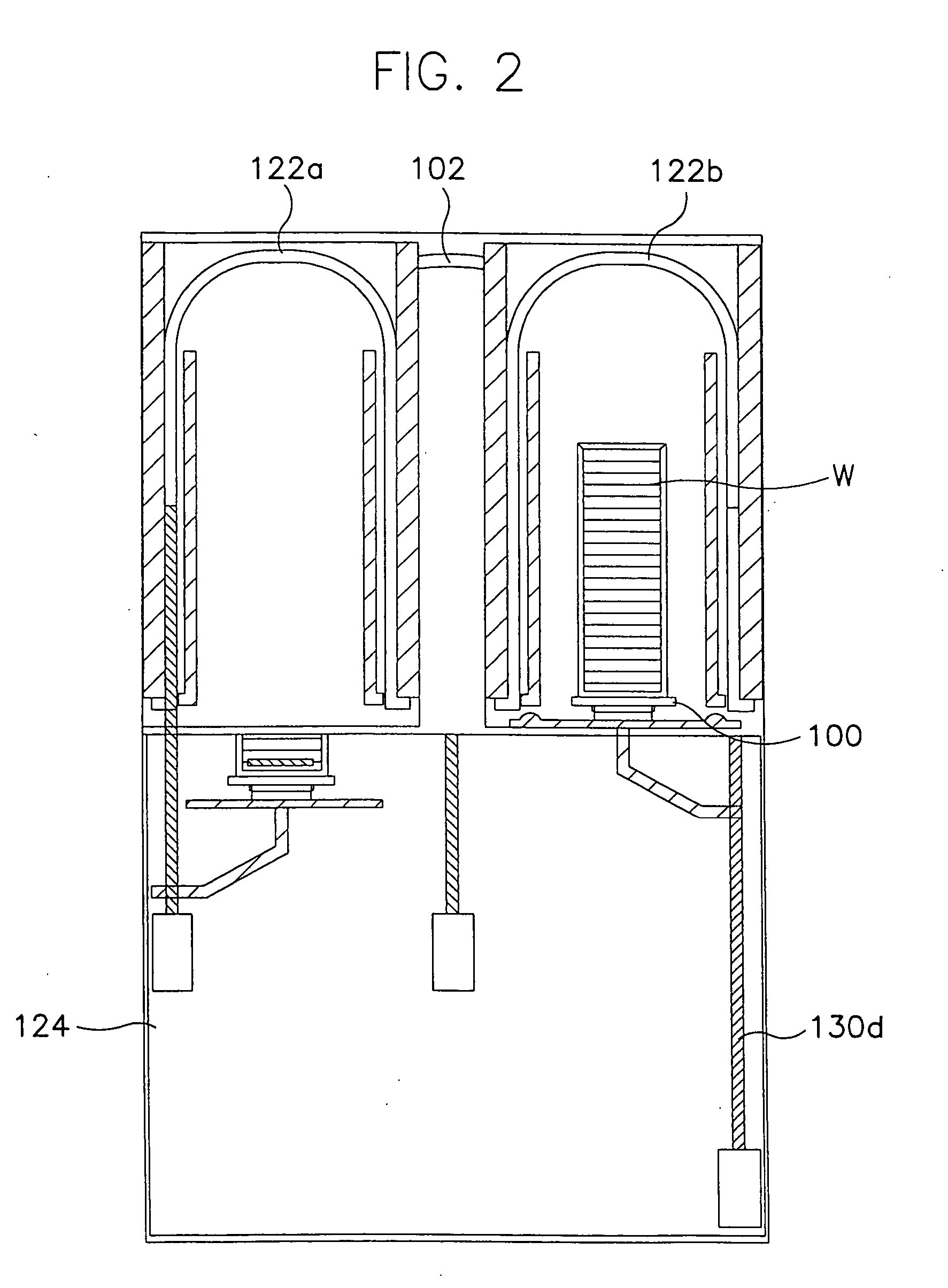
[0028] First, the semiconductor processing apparatus according to the present invention will be described with reference to FIGS. 2 to 5.
[0029] The semiconductor processing apparatus includes a boat 100 for receiving a plurality of sheets of wafers. The boat 100 can receive 25 sheets to 100 sheets of wafers, constituting one process group or batch of wafers. The apparatus also includes a dry etch module 102 for performing a dry etch process on a batch of wafers. The dry etch module 102 removes native oxide from the surfaces of the wafers. The dry etch module 102 will now be described in detail with reference to FIG. 5.
[0030] The dry etch module 102 comprises an etching chamber 104 having a volume capable of receiving the boat 100 on which the plurality of sheets of wafers are mounted. An inlet through which the boat 100 is introduced into the c...
PUM
| Property | Measurement | Unit |
|---|---|---|
| temperature | aaaaa | aaaaa |
| temperature | aaaaa | aaaaa |
| time | aaaaa | aaaaa |
Abstract
Description
Claims
Application Information