Method of and apparatus for performing sequential processes requiring different amounts of time in the manufacturing of semiconductor devices

a technology of sequential process and semiconductor device, which is applied in the direction of lighting and heating apparatus, charge manipulation, furnaces, etc., can solve the problems of undesired native oxide growing on the surface of the wafer, affecting the production efficiency of the respective unit process, and affecting the production efficiency of the respective unit. achieve the effect of high production efficiency, high efficiency and no significant downtim

Inactive Publication Date: 2005-06-28
SAMSUNG ELECTRONICS CO LTD
View PDF11 Cites 223 Cited by
  • Summary
  • Abstract
  • Description
  • Claims
  • Application Information

AI Technical Summary

Benefits of technology

[0016]That is, one object of the present invention is to provide a method of manufacturing a semiconductor device that includes first and second processes requiring different processing times and yet is both highly productive and highly efficient. Likewise, an object of the present invention is to provide an apparatus capable of performing the semiconductor manufacturing process without producing devices prone to process failures and without the need for significant downtime.

Problems solved by technology

However, productivity still lags in many areas of the manufacturing process and the respective unit processes are still prone to failures having a certain root cause.
In other words, an undesired native oxide is grown on the surface of the wafer before the actual CVD process begins.
Accordingly, a film is formed on the native oxide and not on the surface of the wafer, whereby a process failure will occur.
This increase in the contact resistance results in a corresponding decrease in the operation speed of the semiconductor device and otherwise degrades the electrical properties and reliability of the device.
However, the mass production of semiconductor devices makes it very difficult to perform the deposition process directly after the wet etch process.
Also, incorporating the wet etch process into the overall manufacturing process reduces the manufacturing rate because the wet etch process equipment and the deposition process equipment are separately operated.
Moreover, a native oxide cannot be completely prevented from re-growing on the surface of the wafer even when the deposition process is performed within the time period called for, by the process recipe, after the native oxide is removed.
Thus, it is very difficult to use wet etching to prevent a native oxide from residing on the surface of the wafer before the CVD process is initiated.
However, this process requires a great deal of time because the apparatus uses a robot arm to transfer the wafers from the loadlock chamber.

Method used


Image

  • Method of and apparatus for performing sequential processes requiring different amounts of time in the manufacturing of semiconductor devices
  • Method of and apparatus for performing sequential processes requiring different amounts of time in the manufacturing of semiconductor devices
  • Method of and apparatus for performing sequential processes requiring different amounts of time in the manufacturing of semiconductor devices

Examples


Embodiment Construction

[0027]The preferred embodiments of the present invention will hereinafter be described in detail with reference to accompanying drawings.

[0028]First, the semiconductor processing apparatus according to the present invention will be described with reference to FIGS. 2 to 5.

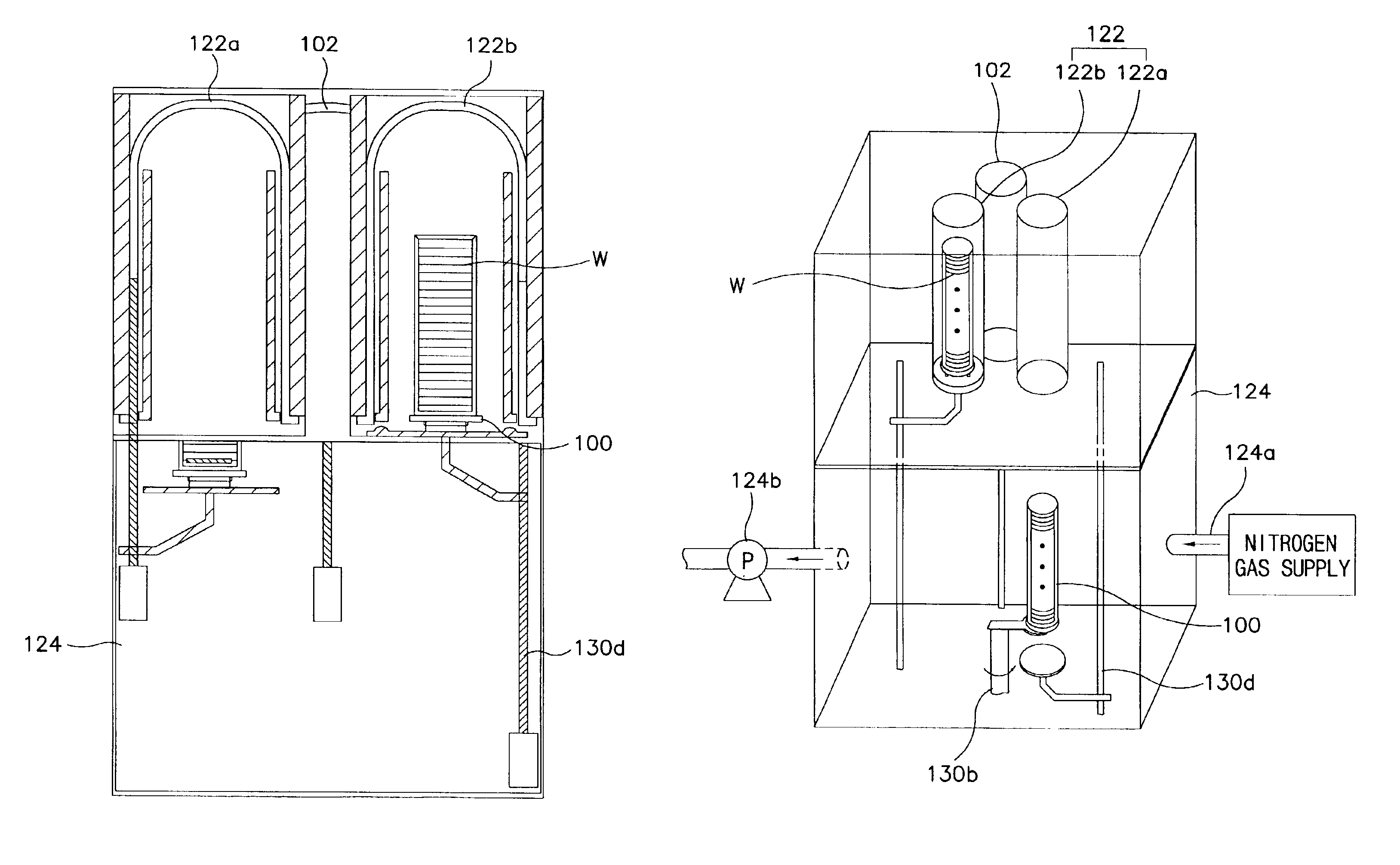
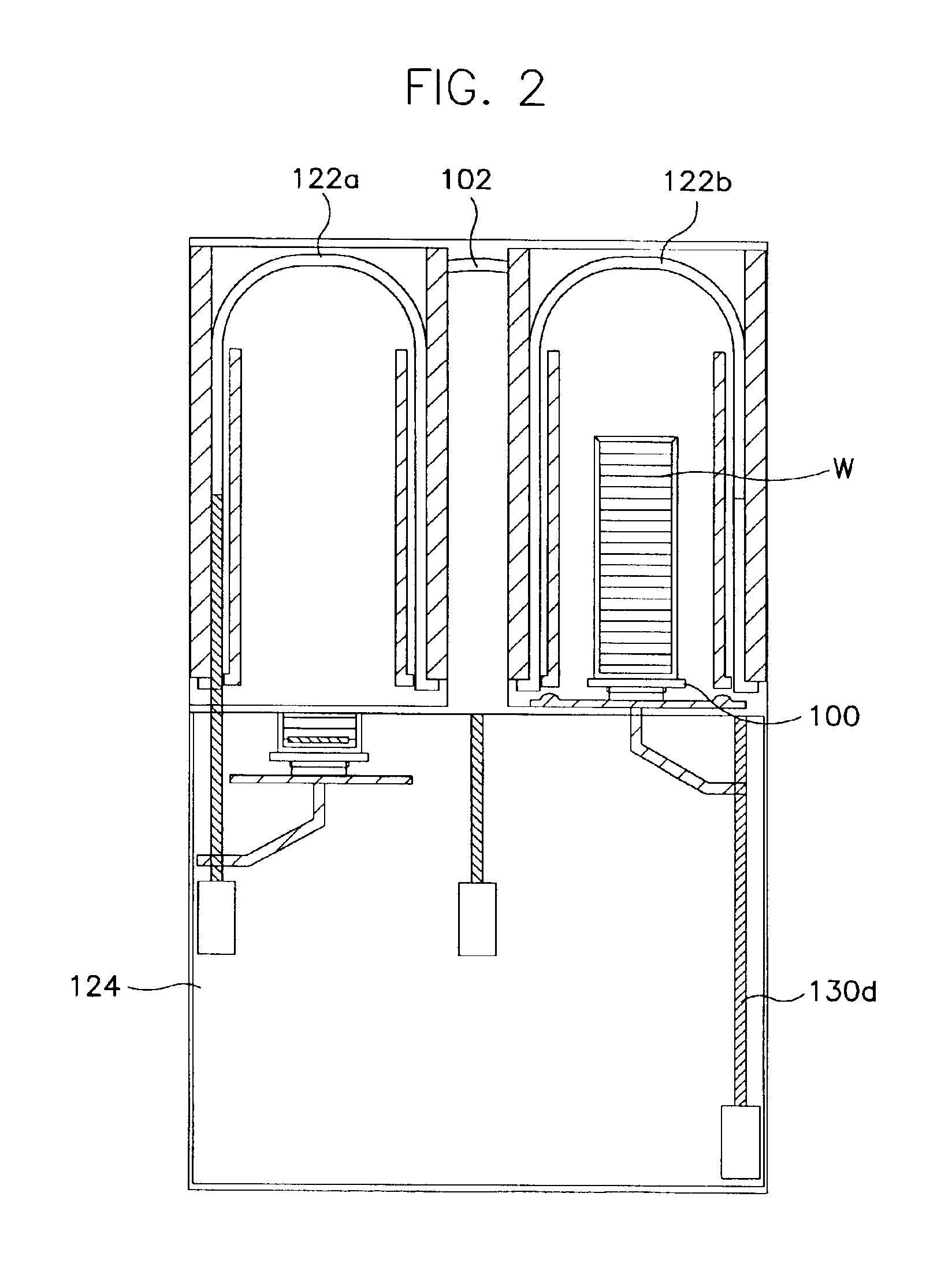
[0029]The semiconductor processing apparatus includes a boat 100 for receiving a plurality of sheets of wafers. The boat 100 can receive 25 sheets to 100 sheets of wafers, constituting one process group or batch of wafers. The apparatus also includes a dry etch module 102 for performing a dry etch process on a batch of wafers. The dry etch module 102 removes native oxide from the surfaces of the wafers. The dry etch module 102 will now be described in detail with reference to FIG. 5.

[0030]The dry etch module 102 comprises an etching chamber 104 having a volume capable of receiving the boat 100 on which the plurality of sheets of wafers are mounted. An inlet through which the boat 100 is introduced into the chamber ...


PUM

PropertyMeasurementUnit
timeaaaaaaaaaa
temperatureaaaaaaaaaa

Abstract

A method of manufacturing a semiconductor device includes first and second processes, the latter requiring more processing time. An apparatus for performing the semiconductor manufacturing process includes a first reactor, and a plurality of second reactors for each first reactor. A first group of wafers are subjected to the first process within the first reactor, and are then transferred into a second reactor as isolated from the outside air. The first group of wafers is subjected to the second process within the second reactor. At the same time, a second group of wafers are subjected to the first process within the first reactor. After the first process is completed, the second group of wafers is transferred into an unoccupied one of the second reactors as isolated from the outside air. There, the second group of wafers is subjected to the second process. Accordingly, process failures otherwise due to the exposure of the wafers are minimized, and productivity is high despite the difference in the processing times.

Description

BACKGROUND OF THE INVENTION[0001]1. Field of the Invention[0002]The present invention relates to a method of and apparatus for manufacturing semiconductor devices. More particularly, the present invention relates to a method of and apparatus for forming a film on a plurality of wafers.[0003]2. Description of the Related Art[0004]Generally, semiconductor devices are manufactured by repeatedly performing a series of processes, such as photolithography, etching, ion implantation, chemical and mechanical polishing and the like, on a wafer. The respective conditions under which these processes are performed must be optimized such that the semiconductor devices manufactured by the unit processes have enhanced functions and a minimal rate of failure. In addition, the time periods under which the respective processes are carried out should be optimized so as to enhance the productivity of the overall semiconductor device manufacturing process.[0005]The respective unit processes have been gr...

Claims


Application Information

Patent Timeline
Patent Type & Authority Patents(United States)
IPC IPC(8): C23C16/02C23C16/54H01L21/00H01L21/311H01L21/02
CPCC23C16/0236C23C16/54H01L21/67276H01L21/31116Y10S414/139H01L21/02
Inventor AN, JAE-HYUCK
Owner SAMSUNG ELECTRONICS CO LTD
Why Eureka
Try Eureka