Method and apparatus for illuminating a substrate during inspection

a substrate and inspection method technology, applied in the direction of optical radiation measurement, instruments, spectrometry/spectrophotometry/monochromators, etc., can solve the problems of system drawbacks, shrinking of semiconductor line widths, and increasing of semiconductor wafer yield losses, so as to facilitate optical inspection of a surface, facilitate the illumination of a predefined portion, and facilitate the effect of optical inspection

Inactive Publication Date: 2005-07-07
TWINSTAR SYST +1
View PDF1 Cites 25 Cited by
  • Summary
  • Abstract
  • Description
  • Claims
  • Application Information

AI Technical Summary

Benefits of technology

[0008] As an optical inspection system, one embodiment of the invention comprises a light source configured to emit light along an illumination path so as to facilitate optical inspection of a surface of a semiconductor wafer. The invention also includes a reflector configured to reflect the illumination path onto the semiconductor wafer. An optically opaque filter is placed in the illumination path between the light source and the reflector, this filter having an aperture shaped so as to pass a portion of the light along the illumination path on to the reflector so as to generate a predefined illuminated area on the surface of the semiconductor wafer.
[0009] As an apparatus for shaping a light path in an optical inspection system, another embodiment of the invention comprises an optically opaque body configured for placement within a light path of an optical inspection system and at an incidence an

Problems solved by technology

As pressure to increase chip performance causes semiconductor line widths to shrink, semiconductor wafer yield losses are increasing due to pattern defects.
Such systems suffer from certain drawbacks, however.
However, it is difficult to project a light beam at an angle while still generating a circular illumination field on the substrate, so as to illuminate the wafer up to its edges, but not beyond.
Illumination beyond the wafer edge is problematic, as it can cause light to scatter with high intensity, masking scattered light from defects.
In doing so, the edges 4 of the wafer 6 are illuminated, where fabricati

Method used


Image

  • Method and apparatus for illuminating a substrate during inspection
  • Method and apparatus for illuminating a substrate during inspection
  • Method and apparatus for illuminating a substrate during inspection

Examples


Embodiment Construction

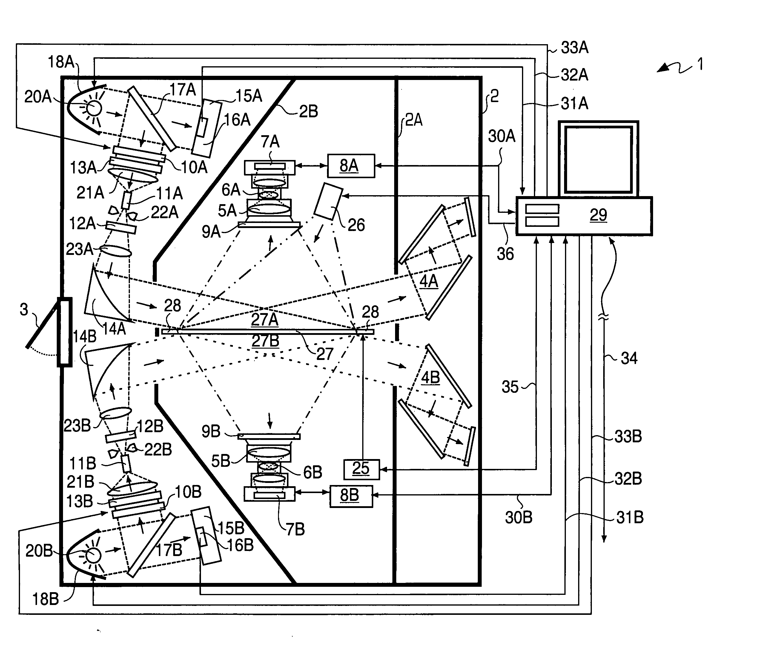
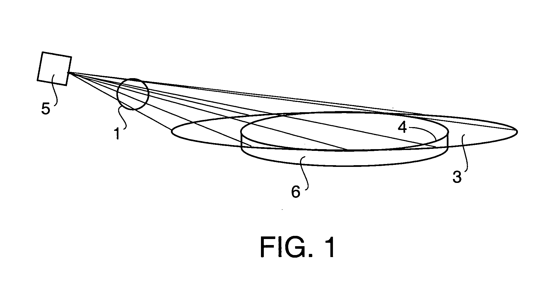
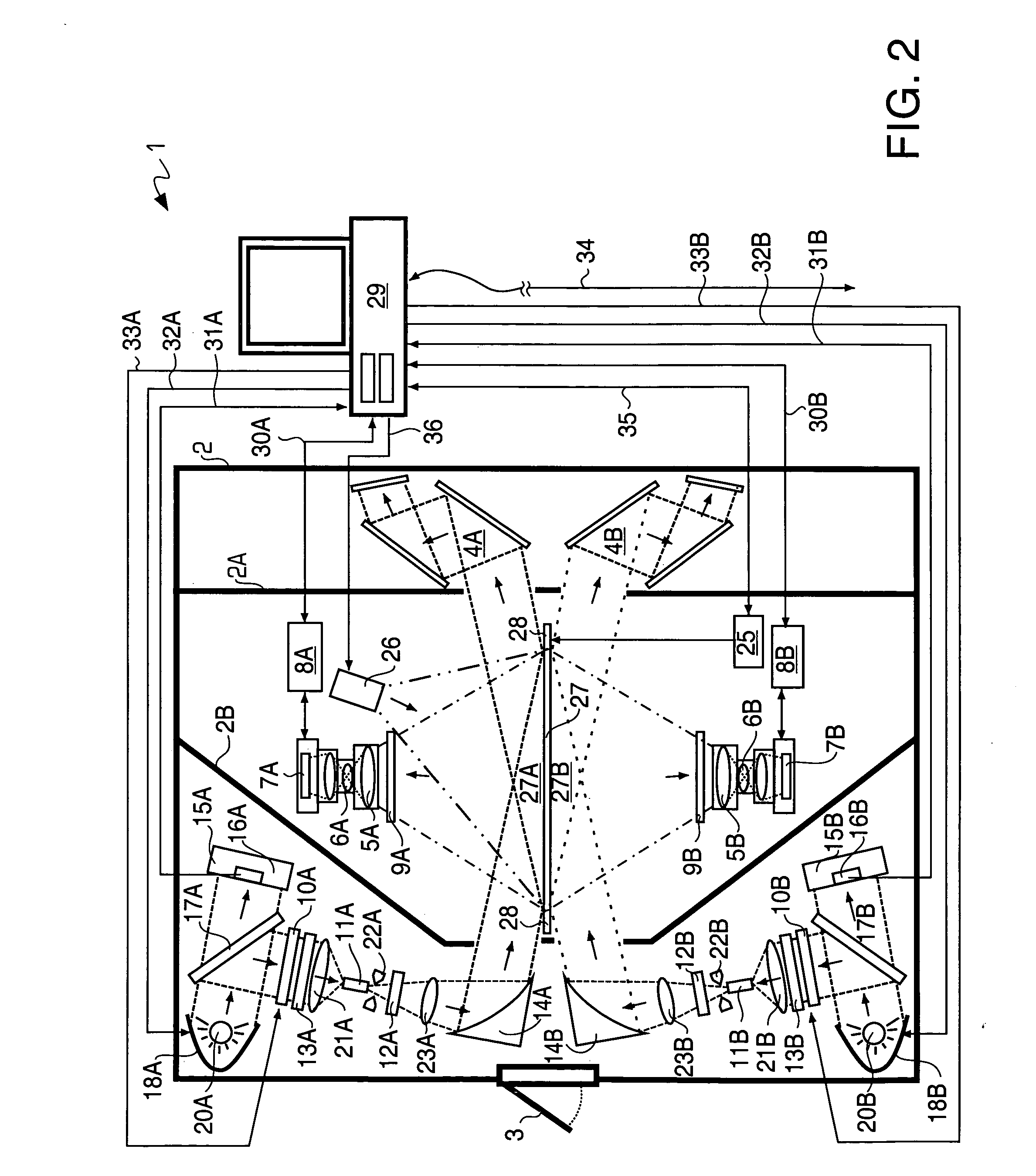
[0026] In one sense, the invention relates to the projection of a light field on a substrate, the light field having a uniform intensity across the substrate, as well as a predefined area with sharp edge cutoff. To illuminate a specific predefined area, an aperture is placed within a light beam path. This aperture has a specifically designed three-dimensional profile, so as to shape the light beam in a specific manner. When this shaped light beam is transmitted through the appropriate optics, its profile is altered so as to be projected onto the wafer as a circle (or any other desired shape) with sharp cutoff edges. The invention also includes methods of designing aperture profiles to produce any specific desired shape of the substrate illumination area with sharp edge cutoff. In this manner, given any predetermined shape of the area to be illuminated, the invention allows the design of an appropriate aperture for generating that shape, even when the light path must first be focused...


PUM


Abstract

Projection of a light field on a semiconductor wafer, the light field having uniform intensity and a predefined area. An aperture is placed within a light beam path, with a specifically designed three-dimensional profile, so as to shape the light beam in a specific manner. When this light beam is transmitted through the appropriate optics, its shape is altered so as to be projected onto the wafer as a circle (or any other desired shape). An optical mask is also employed, with a varying light attenuation to impart a varying intensity to the light path. The aperture shapes the light path, and the optical mask selectively attenuates it, in so that the end result is a uniformly-intense light field that illuminates only a specific predefined area of the wafer. Wafers can thus be illuminated while avoiding undesirable areas such as wafer edges, thus preventing over- or under-illumination.

Description

[0001] This application claims priority to International Application Number PCT / US2003 / 031071, which was filed on 26 Sep. 2003, and which in turn claims priority to U.S. Provisional Patent Application No. 60 / 414,511, which was filed on 27 Sep. 2002, and U.S. patent application Ser. No. 10 / 672,056, which was filed on 25 Sep. 2003.BRIEF DESCRIPTION OF THE INVENTION [0002] This invention relates to optical inspection of substrates. More specifically, this invention relates to the illumination of substrates during optical inspection. BACKGROUND OF THE INVENTION [0003] As pressure to increase chip performance causes semiconductor line widths to shrink, semiconductor wafer yield losses are increasing due to pattern defects. Pattern defects, such as pattern misregistration, extra features, and missing features in patterns, can vary in size. Defects of approximately 0.035 um and above can be detected by known optical imaging methods, depending on factors such as the presence of patterns. Sm...

Claims


Application Information

Patent Timeline
IPC IPC(8): G01J3/10G01N21/47G01N21/94G01N21/95
CPCG01J3/10G01N21/9501G01N21/94G01N21/47
Inventor CHHIBBER, RAJESHWARWILLENBORG, DAVID
Owner TWINSTAR SYST
Why Eureka
Try Eureka