Active-matrix type display device

Inactive Publication Date: 2005-04-26
RENESAS ELECTRONICS CORP
View PDF7 Cites 151 Cited by
  • Summary
  • Abstract
  • Description
  • Claims
  • Application Information

AI Technical Summary

Benefits of technology

[0045]With the above configuration, the time during which displayed contents are not changed exceeds the specified time, the luminance is decreased for each of the pixels, each of the lines or each of the frames and also the luminance is made low in the pixel, line or frame for which bright displaying is not required and therefore the power consumption can be greatly reduced.
[0046]With another configuration, the current that flows through the EL device making up the pixel of the image having less importance is made small and therefore the power consumption can be also lowered greatly.
[0047]With still another configuration, the current that flows throu

Problems solved by technology

When a back light is incorporated into the liquid crystal display, luminance on an entire screen is increased, thus presenting a problem in that the liquid crystal display consumes much power.
Though structure of the simple-matrix type organic EL display device is comparatively simple and its manufacturing costs can be reduced, it is difficult to increase the number of pixels and difficult to achieve a high definition display device.
To maintain the luminance at a specified level within limited time, it is necessary to instantly pass a large electric current through each of the pixels, which presents basic problems in that the luminance becomes low as accumulated emissive time is lengthened and a life of emissive material is shortened due to flowing of such the large electric current as the driving current through the simple-matrix type organic EL display device.
Since the organic EL display device is a current-driven type display device, the TFT adapted to simply perform ON/OFF operations such as those used in the active-matrix type liquid crystal display device cannot be used and the TFT having on-resistance being small enough to pass sufficient currents is required.
Su

Method used


Image

  • Active-matrix type display device
  • Active-matrix type display device
  • Active-matrix type display device

Examples


first embodiment

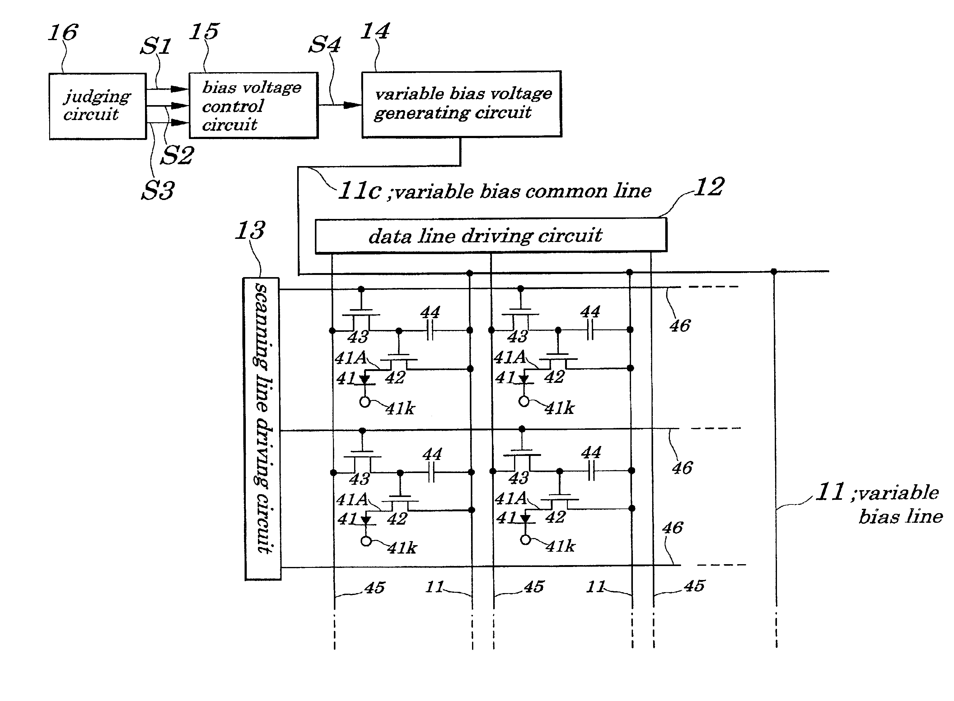
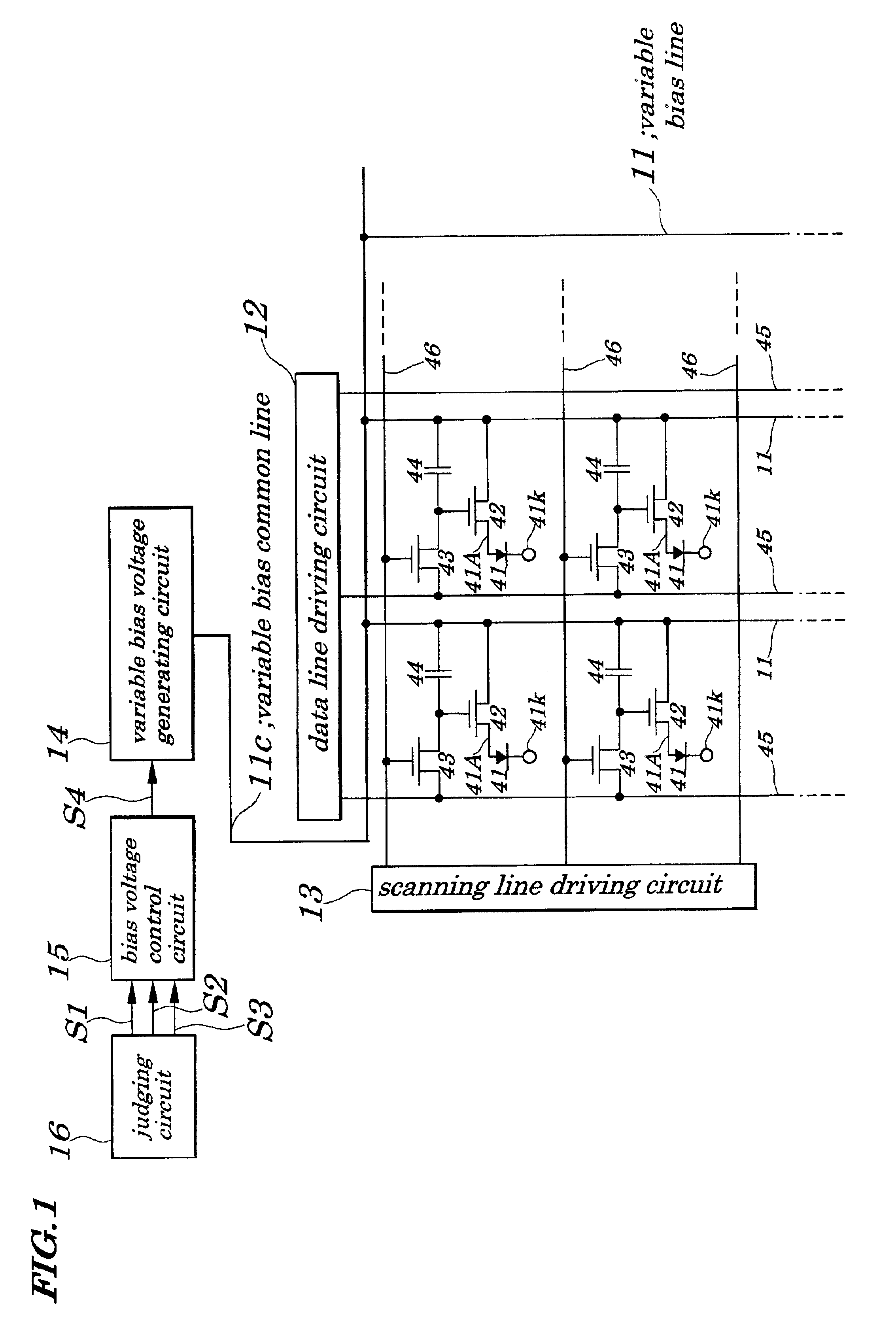
[0055]FIG. 1 is a schematic block diagram of a display device according to a first embodiment of the present invention. In FIG. 1, same reference numbers as those in FIG. 4 are assigned to corresponding parts having the same functions as those in FIG. 4. The display device of the embodiment shown in FIG. 1 includes an EL device 41 having an anode 41A and a cathode 41K biased so as to be at a specified voltage, a TFT 42 connected between the anode of the EL device 41 and a variable bias line 11, a TFT 43 connected between a gate of the TFT 42 and a data line 45 and operated as a switch, and a capacitor 44 connected between the gate of the TFT 42 and the variable bias line 11, which are arranged in a matrix form.

[0056]The display device of the embodiment is provided with a data line driving circuit 12 used to drive the data line 45, a scanning line driving circuit 13 used to drive a scanning line 46, and a variable bias voltage generating circuit 14 used to drive the variable bias lin...

second embodiment

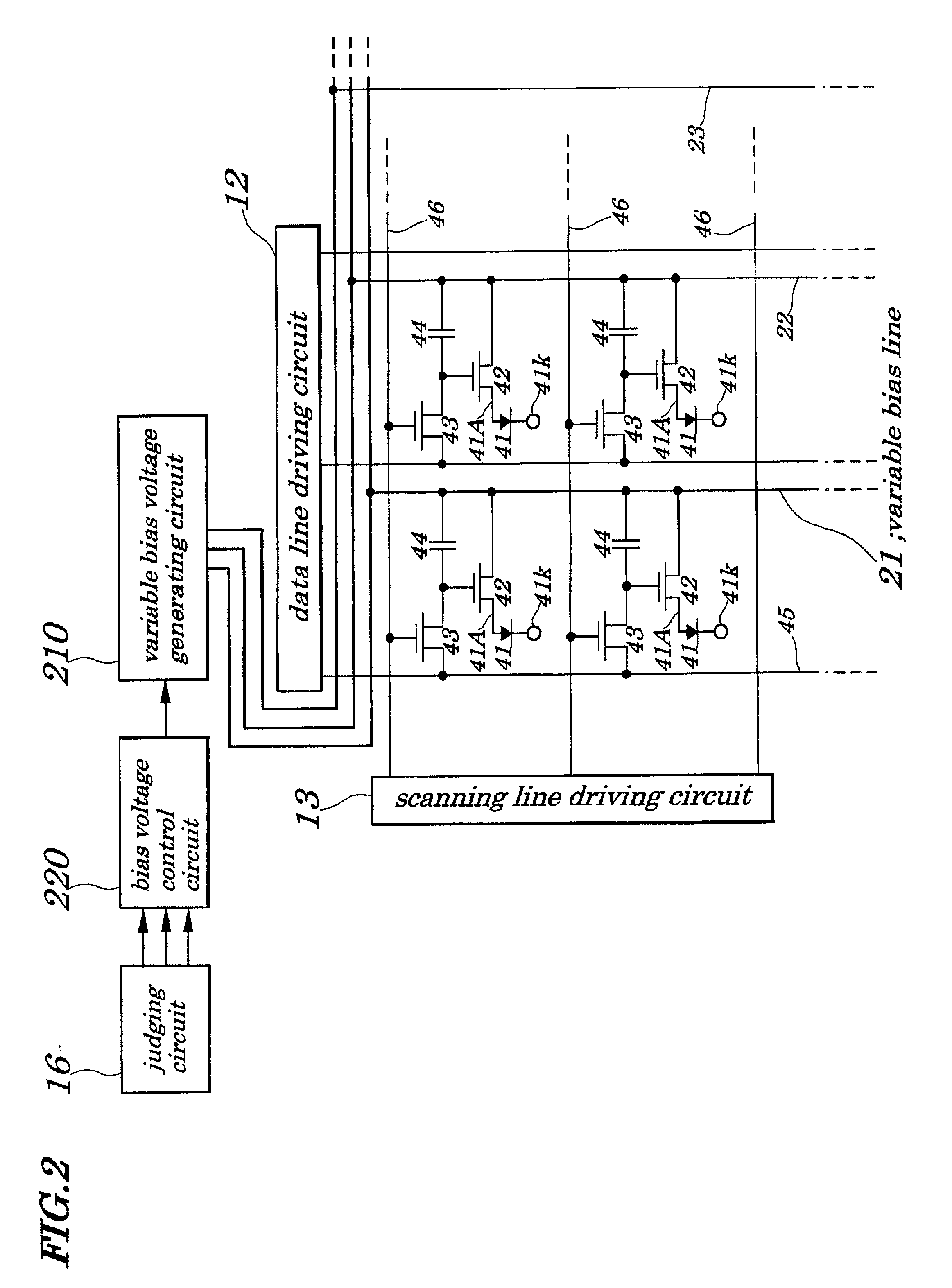
[0076]FIG. 2 is a schematic block diagram of a display device according to a second embodiment of the present invention. In FIG. 2, same reference numbers as those in FIG. 1 are assigned to corresponding parts having the same functions as those in FIG. 1. In FIG. 1, a variable bias common line 11c which is used as a common line to the variable bias lines 11 making up the display device is connected to one output terminal of a variable bias voltage generating circuit 14, however, in FIG. 2, each of a plurality of variable bias lines 21, 22, 23 to 2N making up the display device is connected to each of different output terminals of variable bias voltage generating circuit 210.

[0077]By configuring as above, currents that flow through an EL device 41 can be simultaneously and independently controlled for one column of the EL devices 41 and, as a result, luminance of one column of the EL devices 41 can be calibrated simultaneously and independently.

[0078]For example, when the display dev...


PUM


Abstract

A display device is provided which is capable of controlling luminance of a pixel by a bias voltage of a light emitting device making up the pixel to change a current that flows through the light emitting device.
EL (ElectroLuminescent) devices, TFTs, data lines, scanning lines, and variable bias lines are disposed in a matrix form. A bias voltage control circuit, in response to judging information fed from a judging circuit, outputs control information to a variable voltage generating circuit. The variable voltage generating circuit, in response to the control information, controls currents that are passed through the variable bias line to the EL device so that the EL device emits light at a value of the luminance corresponding to the fed current.

Description

BACKGROUND OF THE INVENTION[0001]1. Field of the Invention[0002]The present invention relates to an active-matrix type display device having an active element and more particularly to the active-matrix type display device having a self-emissive type device such as an organic EL (Electro-Luminescent) device.[0003]The present application claims priority of Japanese Patent Application No.2000-217907 filed on Jul. 18, 2000, which is hereby incorporated by reference.[0004]2. Description of the Related Art[0005]In recent years, portable information terminals have become widespread rapidly as typified by i-mode portable cellular phones (i-mode is a trademark of NTT DOCOMO company) and, as a display device for such the portable information terminals, a liquid crystal display is widely used.[0006]When a back light is incorporated into the liquid crystal display, luminance on an entire screen is increased, thus presenting a problem in that the liquid crystal display consumes much power. To so...

Claims


Application Information

Patent Timeline
IPC IPC(8): G09G3/32G09G3/20H01L51/50G09G3/30G09G5/02H04M1/73
CPCG09G3/2014G09G3/3258H04W52/027G09G5/02G09G2300/0417G09G2320/029G09G2320/043G09G2320/048G09G2330/021G09G2300/0842Y02D30/70
Inventor HASHIMOTO, YOSHIHARU
Owner RENESAS ELECTRONICS CORP
Why Eureka
Try Eureka