Method and apparatus for monitoring tool performance

a tool performance and monitoring method technology, applied in the field of semiconductor processing systems, can solve the problems of deterioration of process data reflecting deterioration of processing characteristics, the difficulty of maintaining and controlling hundreds of complex manufacturing processes and machines, and the constant increase in the cost and tempo of developing new semiconductor devices and building new manufacturing plants

Inactive Publication Date: 2005-08-04
TOKYO ELECTRON LTD
View PDF12 Cites 97 Cited by
  • Summary
  • Abstract
  • Description
  • Claims
  • Application Information

AI Technical Summary

Benefits of technology

[0008] Accordingly, one aspect of the present invention provides a method of monitoring a processing tool in a semiconductor processing system, the method comprising: putting the processing tool into a first state; executing a tool health control strategy; collecting tool health data for the processing tool; executing a tool health analysis strategy; analyzing the tool health data; pausing the processing tool when an alarm has occurred; and refraining from pausing the processing tool when an alarm has not occurred.

Problems solved by technology

The cost and tempo of developing new semiconductor devices and building new manufacturing plants is continually increasing.
Semiconductor manufacturing facilities also face the challenge of maintaining and controlling hundreds of complex manufacturing processes and machines.
Processing conditions change over time with the slightest changes in critical process parameters creating undesirable results.
In many cases, changes of process data reflecting deterioration of processing characteristics cannot be detected by simply referring to the process data displayed.
It is difficult to detect early stage abnormalities and characteristic deterioration of a process.
Inefficient monitoring of a facility can result in facility downtimes that add to the overall operational cost.

Method used


Image

  • Method and apparatus for monitoring tool performance
  • Method and apparatus for monitoring tool performance
  • Method and apparatus for monitoring tool performance

Examples


Embodiment Construction

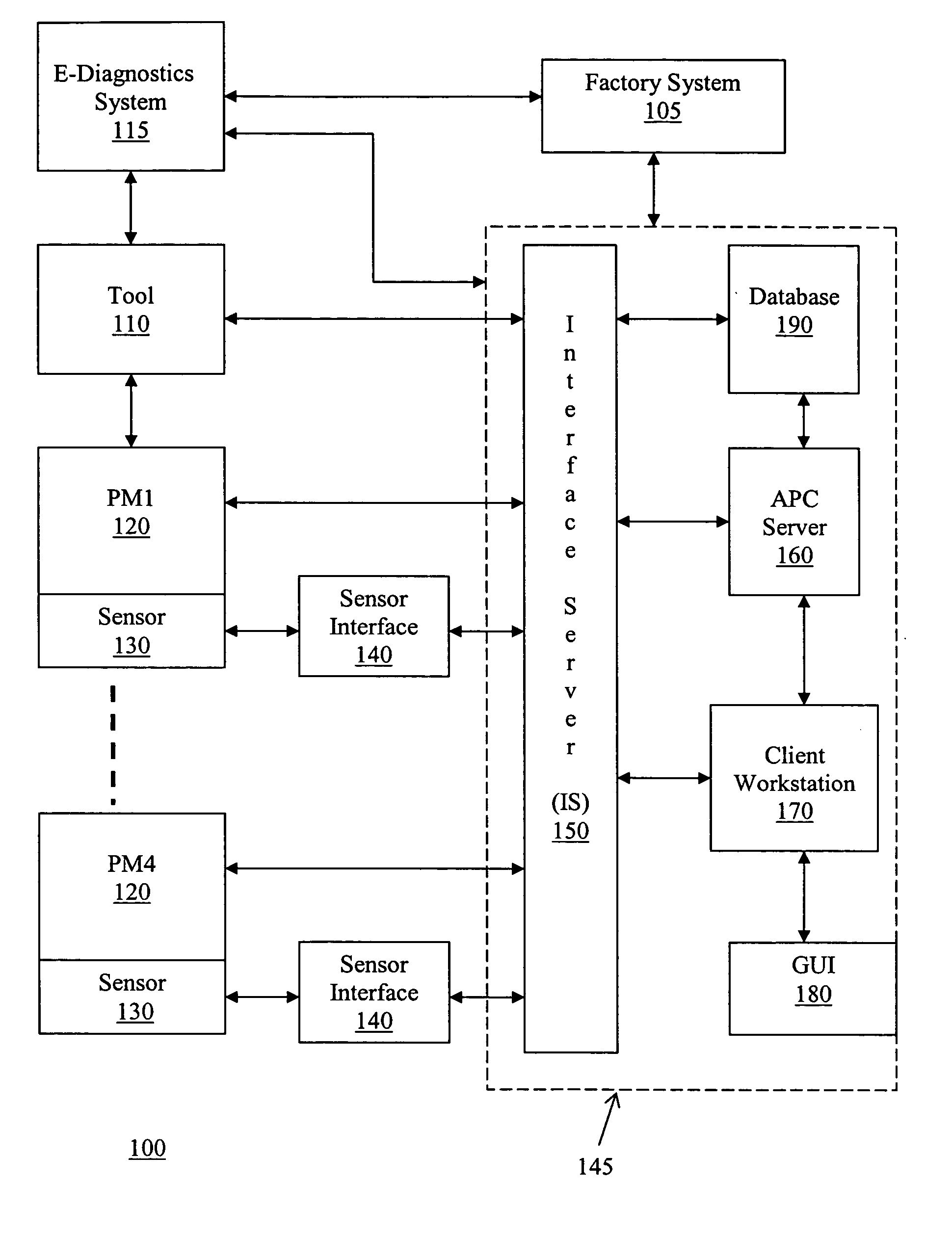
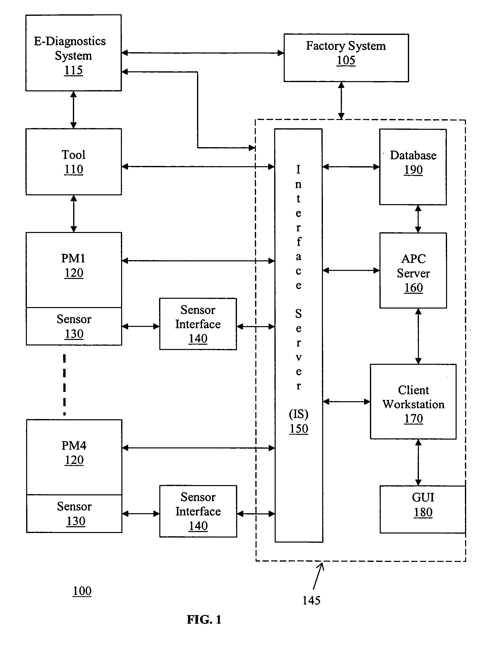
[0036] In semiconductor manufacturing computers are generally used to control, monitor, and setup manufacturing processes. The embodiment described below provides a tool status monitoring system for a semiconductor processing system. The system can include the monitoring of processing tools, processing modules (chambers), and / or sensors, and the management of alarms associated with the tools, modules, and sensors. The embodiment employs a set of computer GUIs that are comprehensible, standardized in format, and simplify the tool status monitoring processes. The graphical displays are organized so that all significant parameters are clearly and logically displayed. GUI screens are provided that allow the user to make changes after system installation.

[0037] The tool status monitoring system can be provided in multiple languages. The page layouts have been designed to support in global installations. Users in many countries will find the tool status monitoring system easy to use and ...


PUM


Abstract

A method and system for monitoring tool performance for processing tools in a semiconductor processing system. The semiconductor processing system includes a number of processing tools, a number of processing modules, a number of sensors, and an alarm management system. A tool health control strategy is executed in which tool health data for the processing tool is collected. A tool health analysis strategy is executed in which the tool health data is analyzed. An intervention manager can pause the processing tool when an alarm has occurred. The intervention manager refrains from pausing the processing tool when an alarm has not occurred.

Description

CROSS-REFERENCE TO RELATED APPLICATIONS [0001] This is a continuation application of International Application No. PCT / US03 / 16882, filed on May 28, 2003; which is based on and claims the benefit of Provisional U.S. Patent Application No. 60 / 383,619, filed May 29, 2002, the contents of both of which are incorporated by reference herein in their entireties. [0002] The present application is related to co-pending applications U.S. Provisional Application No. 60 / 368,162, entitled “Method for Interaction With Status and Control Apparatus”, filed on Mar. 29, 2002; and U.S. Provisional Application No. 60 / 374,486, entitled “Method and Apparatus for Simplified System Configuration”, filed on Apr. 23, 2002. Each of these applications is herein incorporated by reference in its entirety.FIELD OF THE INVENTION [0003] The present invention is related to semiconductor processing systems, particularly to semiconductor processing systems, which use Graphical User Interfaces (GUIs) to provide a monit...

Claims


Application Information

Patent Timeline
Patent Type & Authority Applications(United States)
IPC IPC(8): H01L21/02G05B19/4065G06F19/00H01L21/00
CPCG05B19/4065G05B2219/37234H01L21/67276H01L21/67253G05B2219/45031H01L21/00H01L21/02
Inventor FUNK, MERRITTTOZAWA, MASAKI
Owner TOKYO ELECTRON LTD
Why Eureka
Try Eureka