Image display device, method of manufacturing image display device, and manufacturing apparatus

a display device and image technology, applied in the manufacture of electrode systems, discharge tubes luminescnet screens, electrode systems, etc., can solve the problems of uneven sealing, easy lowering positioning accuracy, and inability to steadily couple substrates, so as to speed up the sealing operation of the image display device and stabilize the

Inactive Publication Date: 2005-08-18
KK TOSHIBA
View PDF1 Cites 22 Cited by
  • Summary
  • Abstract
  • Description
  • Claims
  • Application Information

AI Technical Summary

Benefits of technology

[0019] According to the image display device and the manufacturing method arranged in this manner, the electrode is connected electrically to the sealing layer that is previously attached to the envelope, and the envelope is formed by electrically heating the sealing layer through the electrode. Thus, a steady current can be supplied to the sealing layer that is formed of the electrically conductive sealing material, and sealing operation for the image display device can be speeded up and stabilized.

Problems solved by technology

Furthermore, heating or cooling in the sealing process causes the front substrate and the rear substrate to expand thermally, thereby easily lowering the positioning accuracy.
Thus, the sealing involves problems in productivity and properties.
If the current value is not stable, however, the time for meting the electrically conductive sealing material varies depending on each individual envelope, so that the substrates cannot be steadily coupled together.
If the electrically conductive sealing material is excessively heated, the substrates are cracked by the resulting heat.
If the material is not fully melted, in contrast with this, the substrates cannot be coupled satisfactorily, so that a problem arises that the vacuum of the envelope cannot be maintained afterward in an exhaust process, for example.

Method used


Image

  • Image display device, method of manufacturing image display device, and manufacturing apparatus
  • Image display device, method of manufacturing image display device, and manufacturing apparatus
  • Image display device, method of manufacturing image display device, and manufacturing apparatus

Examples


first embodiment

[0089] An FED according to this invention and its manufacturing method will now be described in detail with reference to the drawings.

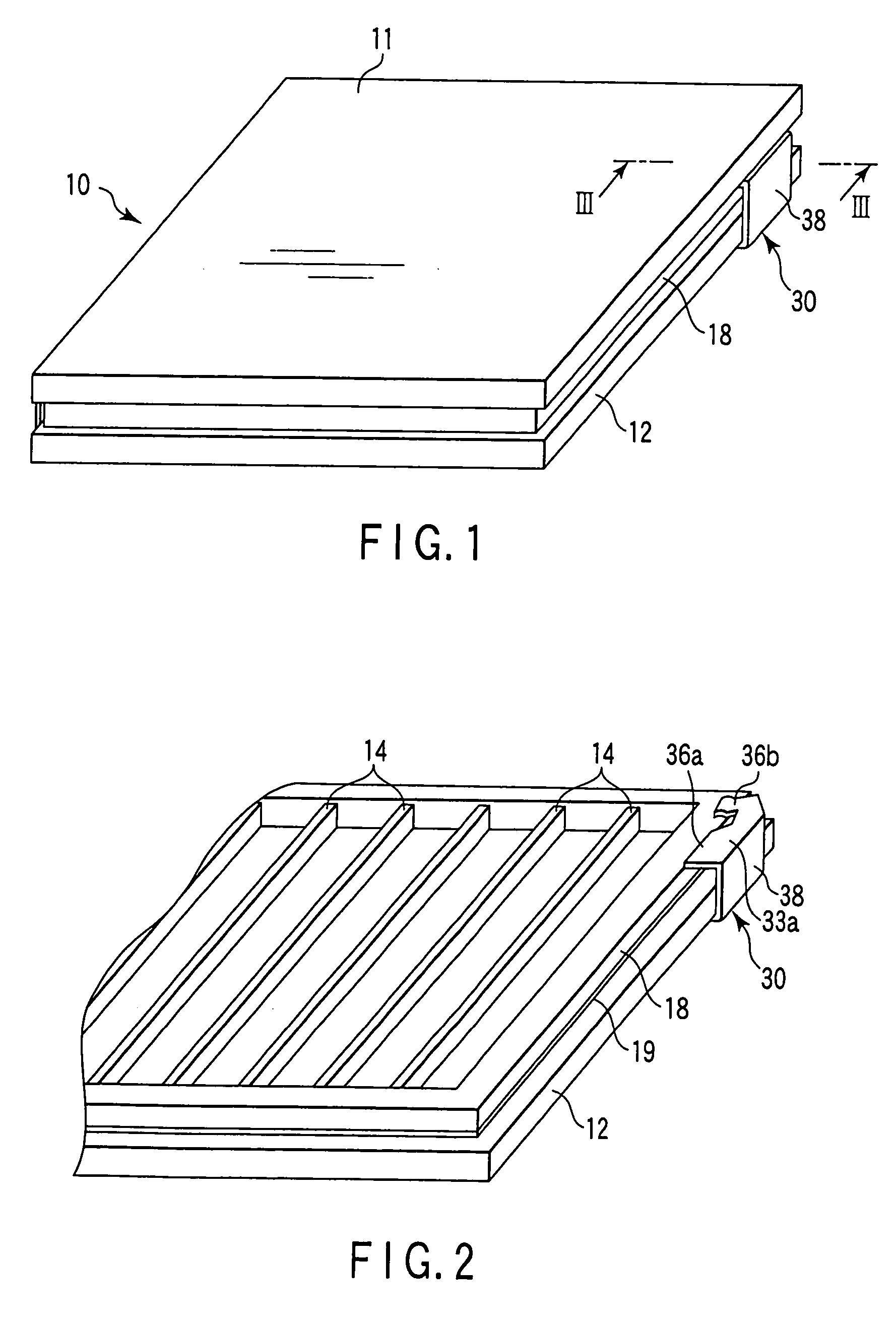
[0090] As shown in FIGS. 1 to 4, the FED comprises a front substrate 11 and a rear substrate 12, which are formed of a rectangular glass sheet each. These substrates are opposed to each other across a gap of about 1 to 2 mm. The front substrate 11 and the rear substrate 12 have their respective peripheral edge portions joined together by a sidewall 18 in the form of a rectangular frame, and constitute a flat, rectangular vacuum envelope 10 that is kept in a vacuum inside.

[0091] A plurality of sheetlike support members 14 are arranged in the vacuum envelope 10 in order to support atmospheric load that acts on the front substrate 11 and the rear substrate 12. These support members 14 individually extend parallel to one side of the vacuum envelope 10 and are arranged at given spaces along a direction perpendicular to the one side. The support members 14...

third embodiment

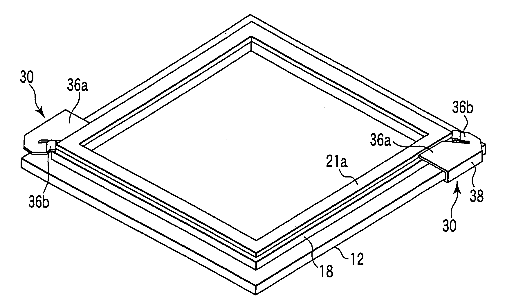
[0120] shown in FIGS. 13, 14A and 14B, an FED is provided with a pair of electrodes 30a, which serve to energize a sealing layer 21a formed on a sidewall 18, and a pair of electrodes 30b, which serve to energize a sealing layer 21b formed on the front substrate 11. The first and second electrodes 30a and 30b, which substantially resemble the aforementioned electrodes 30, are formed in the shape of a clip each. However, each electrode has one contact portion 36.

[0121] The paired first electrodes 30a are attached individually to a pair of corner portions that face each other in the diagonal direction of a rear substrate 12, and are mounted in a manner such that they elastically hold the sidewall 18 and the rear substrate 12 between them. In this case, each first electrode 30a is connected electrically to the sealing layer 21a with its contact portion 36 in contact with the sealing layer. The paired second electrodes 30b are attached individually to a pair of corner portions that face...

fourth embodiment

[0125] The following is a description of an FED according to this invention.

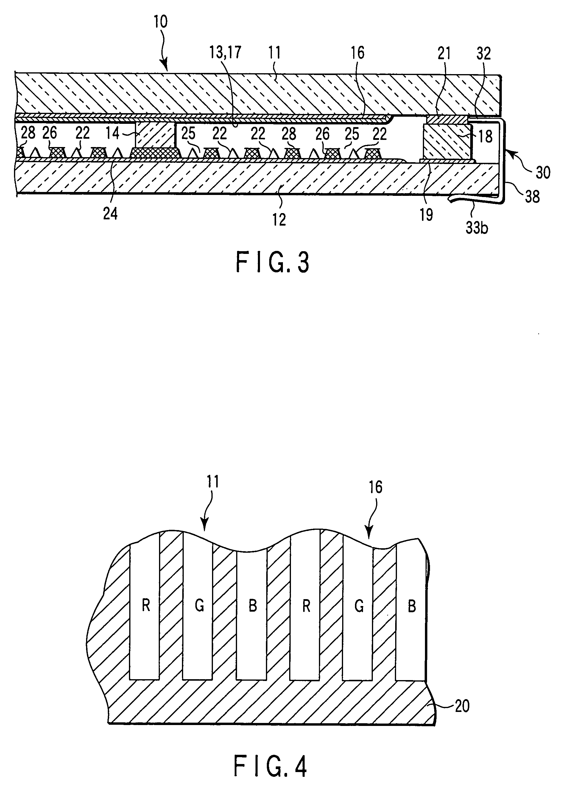
[0126] As shown in FIGS. 15 to 17, the FED is provided with a vacuum envelope 10 and a plurality of, e.g., a pair of, electrodes 30 attached to the vacuum envelope. The vacuum envelope 10 comprises a front substrate 11 and a rear substrate 12, which are formed of a rectangular glass sheet each. These substrates 11 and 12 have their respective peripheral edge portions joined together by a sidewall 18 in the form of a rectangular frame. A phosphor screen 16, a metal back 17, and a getter film 13 are formed on the inner surface of the front substrate 11. A large number of electron emitting elements 22 that excite phosphor layers of the phosphor screen 16 are arranged on the inner surface of the rear substrate 12. Further, a large number of wires 23 that supplies potential to the electron emitting elements 22 are arranged in a matrix on the inner surface of the rear substrate 12, and their respective end portion...


PUM


Abstract

An envelope of an image display device has a front substrate and a rear substrate opposed to the front substrate, and respective peripheral edge portions of the front substrate and the rear substrate are sealed together with a sealing layer which contains an electrically conductive sealing material. An electrode for energizing the sealing layer is attached to the envelope. The electrode is formed of an electrically conductive member, is in electrical contact with the sealing layer, and has a conduction portion exposed to the outside.

Description

CROSS-REFERENCE TO RELATED APPLICATIONS [0001] This is a Continuation Application of PCT Application No. PCT / JP03 / 08929, filed Jul. 14, 2003, which was not published under PCT Article 21(2) in English. [0002] This application is based upon and claims the benefit of priority from prior Japanese Patent Applications No. 2002-206176, filed Jul. 15, 2002; No. 2002-242044, filed Aug. 22, 2002; No. 2002-265757, filed Sep. 11, 2002; No. 2003-004410, filed Jan. 10, 2003; No. 2003-012199, filed Jan. 21, 2003; No. 2003-026227, filed Feb. 3, 2003; No. 2003-141994, filed May 20, 2003; and No. 2003-161034, filed Jun. 5, 2003, the entire contents of all of which are incorporated herein by reference.BACKGROUND OF THE INVENTION [0003] 1. Field of the Invention [0004] This invention relates to a flat image display device having substrates opposed to each other, a method of manufacturing the image display device, and a manufacturing apparatus for the image display device. [0005] 2. Description of the ...

Claims


Application Information

Patent Timeline
Patent Type & Authority Applications(United States)
IPC IPC(8): H01J9/26H01J29/86H01J29/92
CPCH01J9/261H01J29/92H01J29/86
Inventor OKAMOTO, HISAKAZUOOSHIMA, TSUKASAYAMADA, AKIYOSHIENOMOTO, TAKASHIYOKOTA, MASAHIRONISHIMURA, TAKASHIUNNO, HIROTAKATAKEZAWA, HIROHARU
Owner KK TOSHIBA
Why Eureka
Try Eureka