Display element and display apparatus

a display element and display element technology, applied in the field of display elements, can solve the problems of prone to contamination, inability to maintain the charge in the display element, and delay in image display, so as to reduce the degree of change in the entire capacitance of the display element is relatively small, and the concentration of impurity ions is apt to increase.

Inactive Publication Date: 2005-08-18
SHARP KK
View PDF4 Cites 28 Cited by
  • Summary
  • Abstract
  • Description
  • Claims
  • Application Information

AI Technical Summary

Benefits of technology

[0024] However, the display element of the above arrangement has capacitance that monotonously increases as a voltage increases. In this case, a voltage in the display element does not immediately (for example, within one frame) reach a desired voltage, which should reach in response to the voltage application. This causes a problem such as an afterimage in a moving image. Therefore, by providing a region in which the pixel electrode and the counter electrode overlap with each other with the insulating layer therebetween, an auxiliary capacitor is formed parallel to the capacitor of the display element. This can reduce degree of a change in entire capacitance of the display element. This arrangement causes the auxiliary capacitor to be formed parallel to the capacitor of the display element in the equivalent circuit. As a result, the degree of the change in the entire capacitance of the display element becomes relatively smaller. This prevents the problem such as the afterimage in the moving image.
[0025] With the arrangement, a display apparatus including the display element never loses the high-speed response property faster than the response property of the conventional liquid crystal display elements. This allows more secure realization of the high-speed response of the display element that carries out a display by using the change of the medium in terms of magnitude of optical anisotropy.
[0026] Moreover, in the medium of the display element of the arrangement, impurity ion concentration is apt to increase. This decreases specific resistance of the medium. Low specific resistance of the medium decreases luminance of the display element. Moreover, because the specific resistance decreases unevenly on a screen, the luminance accordingly becomes uneven on the screen. However, in the case where the auxiliary capacitor is formed as in the arrangement, it is possible to supply, from the auxiliary capacitor to the medium, an electric charge that corresponds to an electric charge in short (that is, the auxiliary capacitor can supply, to the medium of a part of the screen with which the auxiliary capacitor is associated, electric charge necessary for making up for short of electric charge in the medium). This apparently prevents the decrease in the specific resistance of the medium, and allows an appropriate voltage to be applied to the medium. On this account, it is possible to prevent the decrease in luminance and the unevenness in luminance.
[0027] The present invention ensures (i) realization of the intrinsic high-speed response property of the display element employing the medium, the magnitude of whose optical anisotropy varies according to voltage application, and (ii) prevention of the decrease in the transmittance, and of the unevenness in luminance. This surely improves display response speed of a display apparatus including the display element, for example, display apparatus provided in televisions, word processors, personal computers, video cameras, digital cameras, or information terminals such as mobile phones. On this account, in the display apparatus, it is possible to prevent the decrease in the transmittance and the unevenness in luminance. Further, because the display element of the present invention has the high-speed response property as described above, the display element is suitable for performing a large screen display operation and a moving image display operation.

Problems solved by technology

However, the display element using a material whose optical anisotropy varies according to an applied electric field has the following problems.
Further, in this case, the display element cannot quickly respond to a signal voltage applied through the switching element, thereby causing a delay in image display.
However, in a medium whose optical anisotropy varies according to an applied electric field, the stored charge in the display element does not stay constant after the switching element is switched OFF.
This is because such a medium is apt to be contaminated with impurity ions.
Moreover, because the specific resistance is decreased unevenly in the screen, the luminance becomes uneven on the screen.

Method used


Image

  • Display element and display apparatus
  • Display element and display apparatus
  • Display element and display apparatus

Examples


example 1

Cubic Phase

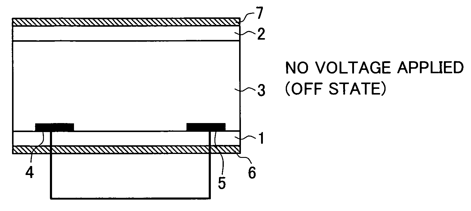
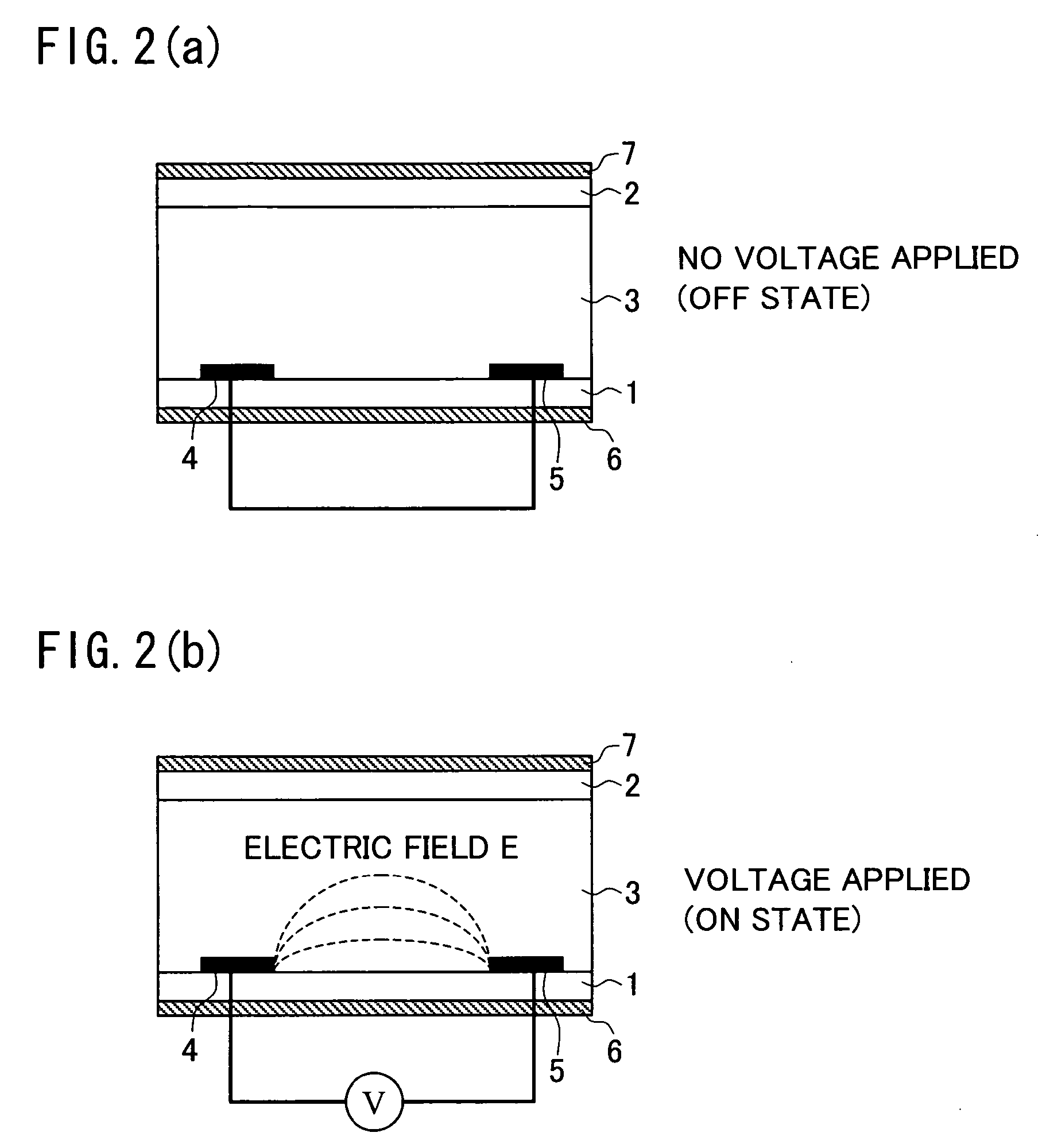
[0132] It is possible to use a medium made of molecules expressing a cubic phase, as the medium injected and sealed in the dielectric material layer 3 of the present display element.

[0133] The material expressing the cubic phase is, for example, BABH8. BABH8 is in the cubic phase in a wide temperature range from 136.7° C. to 161° C., and the stable voltage transmissivity curve can be obtained in the wide temperature range (about 24K). Therefore, it is extremely easy to carry out the temperature control.

[0134] If an electric field is applied to the dielectric material layer 3 made of BABH8 when within the temperature range that BABH8 expresses the cubic phase, the molecules tends to turn in the electric field direction because the molecules have dielectric anisotropy. This causes a distortion of the structure of the minute regions (crystal-like grating). In other words, the dielectric material layer becomes optical anisotropic according to the electric field application...

example 2

Smectic D Phase (SmD)

[0136] As the medium injected and sealed in the dielectric material layer 3 of the present display element, it is possible to apply a medium which is made of molecules in the smectic D phase which is one of the liquid crystal phases.

[0137] One example of liquid crystal materials in the smectic D phase is ANBC16. Note that, ANBC16 is mentioned in Non-patent Document 1 (Kazuya Saito, and Michio Sorai, “Thermodynamics of a unique thermo-tropic liquid crystal having optical isotropy”, Ekisho, 2001, Vol. 5, No. 1 (p.21, FIG.1, Structure 1 (n=16)) and Non-patent Document 6 (“Handbook of Liquid Crystals”, Wiley-VCH, 1998, vol. 2B (p.888, Table 1, Compound No. 1, Compound 1a, Compound 1a-1)). The example includes ANBC etc. represented by the following chemical formulas (2) and (3).

[0138] 4′n-alkoxy-3′-nitro-biphenyl-4-carboxylic acids X═NO2

[0139] n-15 Cr 127 SmC 187 Cub 198 SmA 2041 I

[0140] The liquid crystal material (ANBC16) is in the smectic D phase in a temper...

example 3

Liquid Crystal Microemulsion

[0143] It is possible to apply a liquid crystal microemulsion as the medium injected and sealed in the dielectric material layer 3 of the present display element. The liquid crystal microemulsion is a generic term (named by Yamamoto, et al.) for a system (mixture system) in which oil molecules of O / W type microemulsion (a system in which droplet-shape water is dissolved in oil (continuous phase) by surfactant) are replaced with thermotropic liquid crystal molecules (see Non-patent Document 2: Jun Yamamoto, “Liquid crystal micro emulsion”, Liquid crystal, 2000, Vol. 4, No. 3, pp.248-254).

[0144] A concrete example of the liquid crystal microemulsion is a mixture system of pentylcyanobiphenyl (5CB) mentioned in Non-patent Document 2 and didodecyl ammonium bromide (DDAB) solution. Pentylcyanobiphenyl (5CB) is a thermotropic liquid crystal (temperature transition type liquid crystal) showing a nematic liquid crystal phase, and didodecyl ammonium bromide (DDA...


PUM

PropertyMeasurementUnit
thicknessaaaaaaaaaa
distanceaaaaaaaaaa
widthaaaaaaaaaa

Abstract

A display element includes: a pair of substrates, at least one of which is transparent; a medium, between the substrates, the medium being changeable in an optical anisotropy magnitude by and according to electric field application; and a region in which a pixel electrode and a counter electrode overlap with each other with an insulating layer therebetween.

Description

[0001] This Nonprovisional application claims priority under 35 U.S.C. § 119(a) on Patent Applications Nos. 2004 / 012206 and 2005 / 003221 filed in Japan respectively on Jan. 20, 2004, and on Jan. 7, 2005, the entire contents of which are hereby incorporated by reference. FIELD OF THE INVENTION [0002] The present invention relates to a display element having a high-speed response property, a wide viewing angle property, and a high display quality. BACKGROUND OF THE INVENTION [0003] A liquid crystal display element has advantages over other display elements in terms of thickness, weight, and power consumption, and is therefore widely used for image display apparatuses such as a television set or a monitor; and image display apparatuses provided in: OA (Office Automation) devices such as a word processor or a personal computer; video cameras; digital cameras; and information terminals such as a mobile phone. [0004] There are conventionally well-known liquid crystal display modes for the ...

Claims


Application Information

Patent Timeline
Patent Type & Authority Applications(United States)
IPC IPC(8): G02F1/05G02F1/133G02F1/1343G02F1/1362G02F1/1368G09F9/30G09G3/36
CPCG02F1/136213G02F2201/122G09G3/3611G09G2320/0233G09G3/3651G09G2300/0426G09G3/3629
Inventor MIYACHI, KOICHISHIBAHARA, SEIJIINOUE, IICHIROISHIHARA, SHOICHIKOIDE, TAKAKOOGISHIMA, KIYOSHIJINDA, AKIHITO
Owner SHARP KK
Why Eureka
Try Eureka