Socket for installing electronic parts

Inactive Publication Date: 2005-09-29
SMK CORP
View PDF5 Cites 18 Cited by
  • Summary
  • Abstract
  • Description
  • Claims
  • Application Information

AI Technical Summary

Benefits of technology

[0008] In order to resolve the above-mentioned problems of the prior art, it is an object of the present invention to provide an electronic parts installing socket capable of carrying out satisfactory shielding and capable of downsizing an electronic device by reducing the height of the socket projecting from one surface of the printed circuit board and using spaces of the front and the rear surfaces of the printed circuit board.
[0010] Inasmuch as the electronic parts installing socket according to the first aspect of the present invention comprises a socket housing which is fitted into a socket inserting hole penetrateing from a front surface to a rear surface of a printed circuit board and a plurality of contacts each of which has contact pieces which are held on the socket housing and project from a side surface of the socket housing. The contact pieces are connected in a contact connecting pattern which is positioned at an opening edge portion of the socket inserting hole. Thus, it is possible to reduce the height which projects to one of surfaces of the printed circuit board. As a result, it is possible to downsize the electronic device.
[0011] In addition, inasmuch as the electronic parts installing socket according to the first aspect of the present invention further includes a front surface shielding member for shielding a board front surface of the socket housing and the front surface shielding member having a plurality of shielding pieces which are positioned similar to the teeth of a comb so as to layer the contact pieces of the contacts and which are connected to a shield connecting pattern formed on the opening edge portion of the socket inserting hole. Thus, it is possible to obtain a sufficient shielding effect for the contact pieces and to downsize the electronic device even if surrounding walls of a shielding case are not located at an outside end of the contact pieces.
[0013] As described above, the electronic parts installing socket according to the second aspect of the present invention further has a rear surface shielding member formed in a box shape covering a portion projecting from a rear surface of the printed circuit board to the socket housing. The rear surface shielding member has a plurality of connecting pieces which are arranged similar to the teeth of a comb on an upper edge of the rear surface shielding member and the rear surface shielding member is attached to a rear surface portion of the socket housing. The connecting pieces are connected to the front surface shielding member through the socket inserting hole and the contact pieces of the contacts project outward from gaps between the connecting pieces. As a result, it is possible to sufficiently shield the portion projecting to the rear surface of the printed circuit board together with a portion projecting to the front surface of the printed circuit board. In addition, it is possible to obtain a high shielding efficiency, as the front surface shielding member is connected to the rear surface shielding member.

Problems solved by technology

Heat-sensitive electronic parts are connected to the printed circuit board using an electronic parts installing socket, because it is difficult to install the heat-sensitive electronic parts on the printed circuit board with a soldered connection.
This makes it difficult to downsize the electronic device.
As a result, it is difficult to shrink the electronic device.
In addition, it is difficult to shield a portion which projects from the socket inserting hole of the electronic parts installing socket to the rear surface of the printed circuit board, in the shielding case in which the surrounding wall of the shielding case is located to the outside of the contact piece end.

Method used


Image

  • Socket for installing electronic parts
  • Socket for installing electronic parts
  • Socket for installing electronic parts

Examples


Embodiment Construction

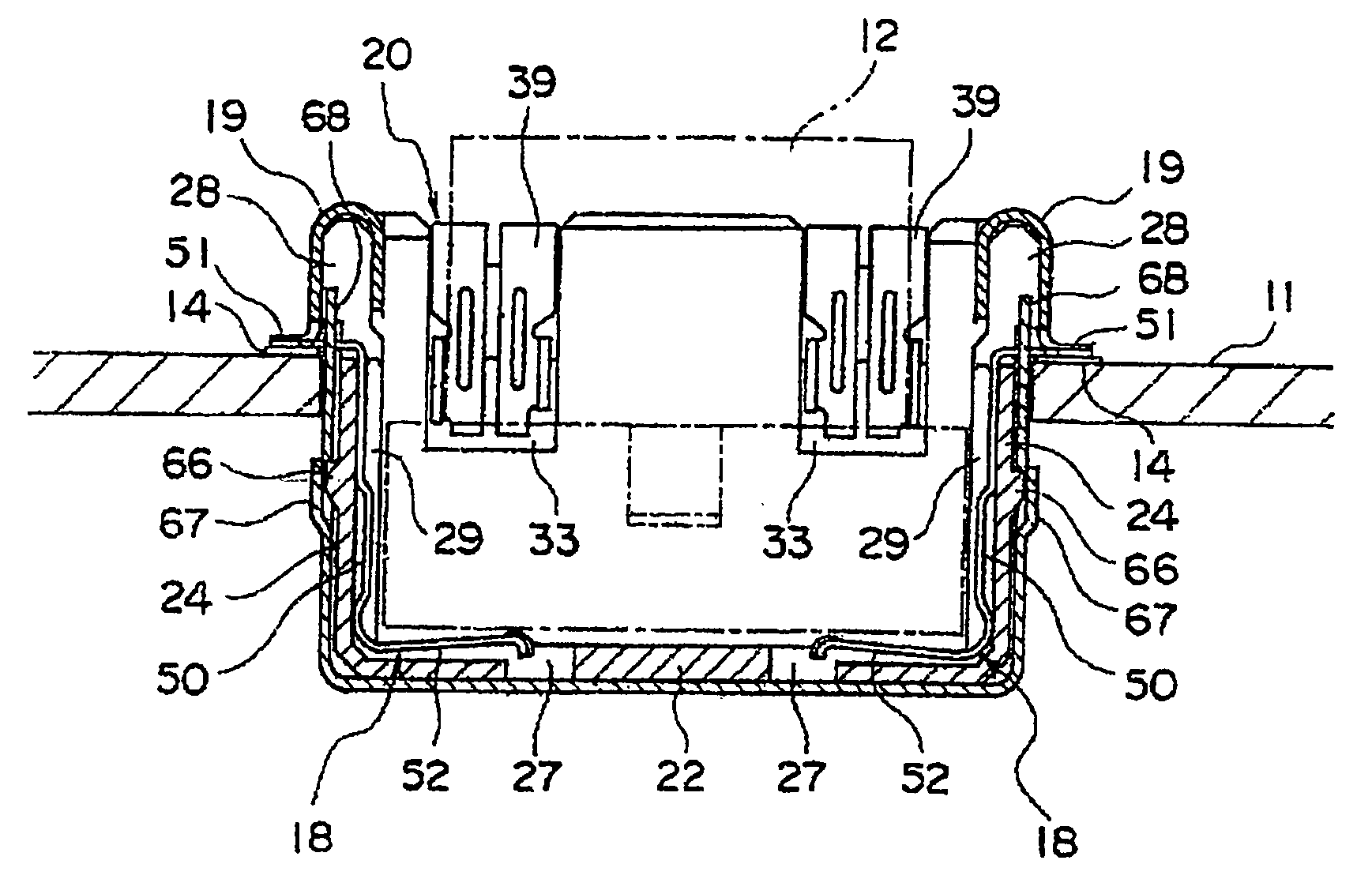
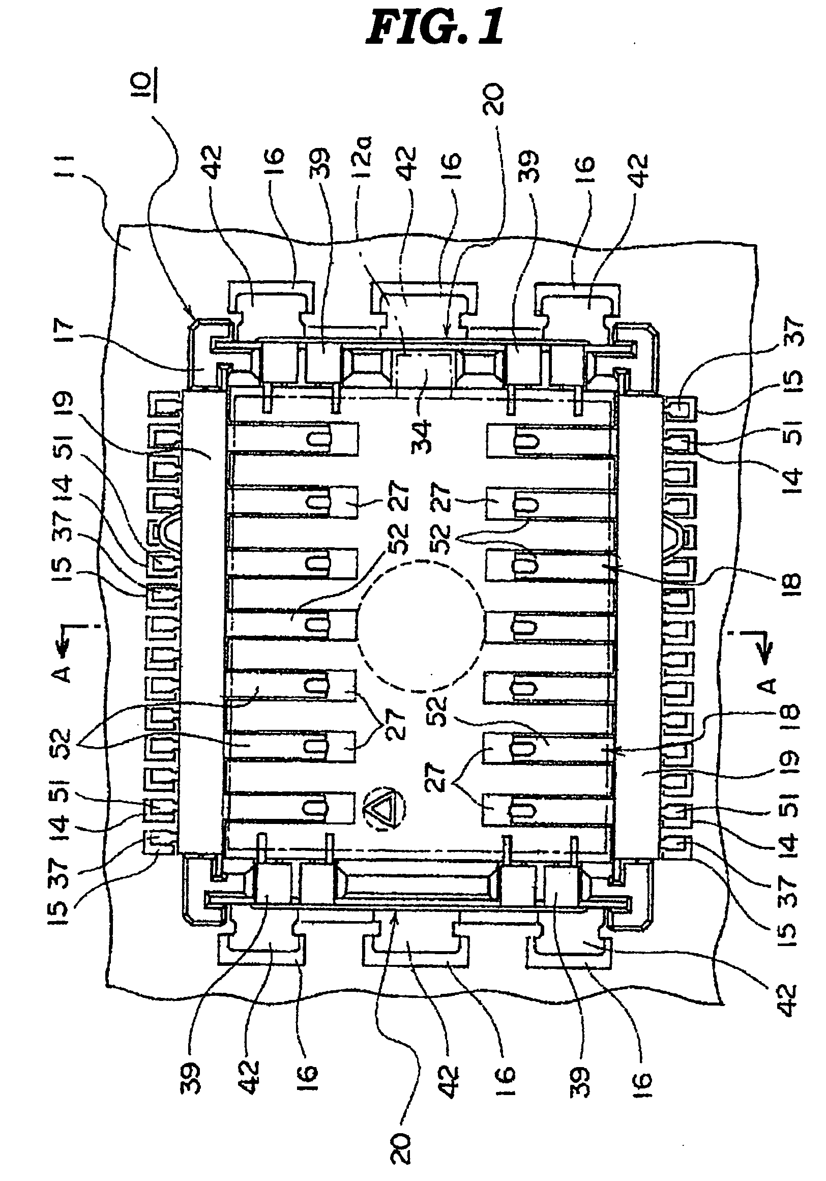
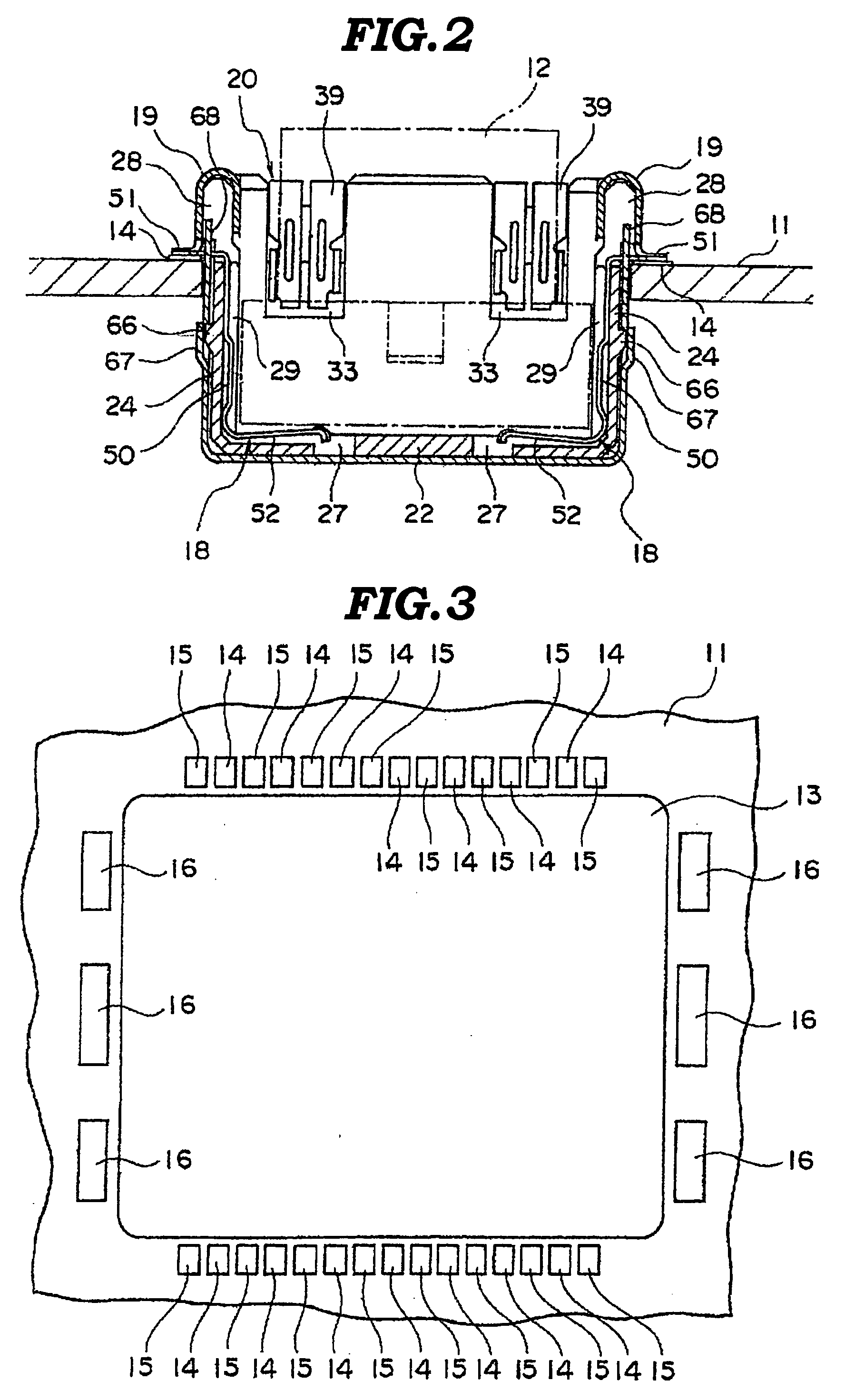
[0035] Description will be made as regards an electronic parts installing socket according to the present invention with reference to FIGS. 1 to 14. FIGS. 1 and 2 illustrate an embodiment in which a camera module is installed on a printed circuit board, using the electronic parts installing socket according to the present invention. The camera module is an example of one of a plurality of electronic parts. FIGS. 1 and 2 illustrate an electronic parts installing socket, a printed circuit board, and a camera module 12 which is one of a plurality of electronic parts.

[0036] As shown in FIG. 3, a socket inserting hole 13 is formed on a predetermined location of the printed circuit board 11. The socket inserting hole 13 penetrates from the front surface to the rear surface of the printed circuit board 11. Contact connecting patterns 14 and shield connecting patterns 15 are located in alternating sequence on a front edge portion and a rear edge portion of the socket inserting hole 13, res...


PUM


Abstract

An electronic parts installing socket capable of downsizing an electronic device by reducing the height of socket projecting from one surface of the printed circuit board comprises a socket housing fitted into a socket inserting hole. The socket inserting hole penetrates from a front surface to a rear surface of a printed circuit board. Also, a plurality of contacts each having contact pieces disposal on the socket housing and project from a side surface of the socket housing. The contact pieces are connected a contact connecting pattern which is positioned at an opening edge portion of socket inserting hole. Front surface shielding members and are connected to the printed circuit board to shield a portion projecting to the front surface of the printed circuit board. A box shaped rear surface shielding member covers a portion projecting from a rear surface of the printed circuit board to the socket housing and is connected to the front surface shielding members.

Description

[0001] The present application claims priority under 35 U.S.C. §119 to Japanese Patent Application No. 2004-088396 filed on Mar. 25, 2004. The content of the application is incorporated herein by reference in its entirety. BACKGROUND OF THE INVENTION [0002] The present invention relates to an electronic parts installing socket for installing electronic parts such as a camera module on a printed circuit board. [0003] Conventionally, an electronic device such as a mobile phone has a printed circuit board in the electronic device. Electronic parts such as a camera module or semiconductor elements are installed on a front surface and a rear surface of the printed circuit board. Heat-sensitive electronic parts are connected to the printed circuit board using an electronic parts installing socket, because it is difficult to install the heat-sensitive electronic parts on the printed circuit board with a soldered connection. [0004] In case of installing the electronic parts on the printed c...

Claims


Application Information

Patent Timeline
IPC IPC(8): H01R24/00H01R12/71H01R12/72H01R13/648H01R13/658H01R13/6595H01R33/76H01R107/00H05K1/18H05K9/00
CPCH05K9/0058H01R12/714H01R13/6595H01R12/728H01R12/721
Inventor ASAI, KIYOSHIKANAZAWA, KAZUAKIKOBAYASHI, JUNICHI
Owner SMK CORP
Why Eureka
Try Eureka