Structure and method to improve channel mobility by gate electrode stress modification

a gate electrode and stress modification technology, applied in the manufacture of transistors, semiconductor devices, electrical equipment, etc., can solve the problems of reduced carrier mobility in deeply scaled bulk mos devices, invariably compromised immutable material properties and physical effects of transistors and other elements, and reduced scale of integrated circuit elements

Inactive Publication Date: 2005-11-03
GLOBALFOUNDRIES INC
View PDF4 Cites 116 Cited by
  • Summary
  • Abstract
  • Description
  • Claims
  • Application Information

AI Technical Summary

Benefits of technology

[0010] It is therefore an object of the present invention to provide a method and structure which can provide tensile and compressive stresses on different electronic element structures on the same chip or wafer.
[0011] It is another object of the invention to provide a method and structure which can be easily and repeatably formed with high manufacturing yield which does not adversely affect the chip or wafer or earlier- or later-conducted manufacturing processes in which tensile and compressive stress levels may be readily controlled.
[0012] It is yet another object of the invention to provide a method and structure which can be relatively free from warping as a result of multiple opposing stresses being alternately applied across a substrate with a net distortion nearing zero.

Problems solved by technology

However, the immutable material properties and physical effects by which transistors and other elements function is invariably compromised as the scale of integrated circuit elements is reduced.
In more recent and critical designs, it has been shown that carrier mobility degrades in deeply scaled bulk MOS devices due to the heavy doping required to suppress short-channel effects and ultra-thin oxide effects.
This phenomenon is well-recognized and theories concerning the physical effects by which it occurs are, in any event, unimportant to its exploitation.
However, there are issues, well known to those skilled in the art, regarding the SiGe-buffer layer or implanted-anneal-buffer approach with a strained Si cap, including dislocations that impact yield severely along with significant trouble containing arsenic diffusion enhancements, cost, and excessive complexity.
Therefore, in integrated circuit designs using both pFET and nFET transistors and CMOS technology (in which the logic is implemented principally by complementary pMOS and nMOS transistor pairs), in particular, an enhancement of carrier mobility on one type of transistor was necessarily accompanied by degradation of carrier mobility in the other or complementary type of transistor; yielding little, if any, net performance gain although theoretically usable to improve symmetry of operation of a CMOS pair.
Moreover, stress of a single type produced by such structures and / or over many areas which may exceed transistor size tends to cause warping or curling of the wafer or substrate which compromises later lithographic processes such as the formation of contacts and connections or, in severe cases, chip or wafer cracking; reducing manufacturing yield or (in rare cases) reliability after being put into service.
Further, the stress levels produced by such structures were generally difficult to control particularly since the structure dimensions are often dictated by other design concerns, such as isolation and breakdown voltages.
Further, such structures may present severe topography on the surface of a chip or wafer which may compromise subsequent manufacturing processes.

Method used


Image

  • Structure and method to improve channel mobility by gate electrode stress modification
  • Structure and method to improve channel mobility by gate electrode stress modification
  • Structure and method to improve channel mobility by gate electrode stress modification

Examples


Embodiment Construction

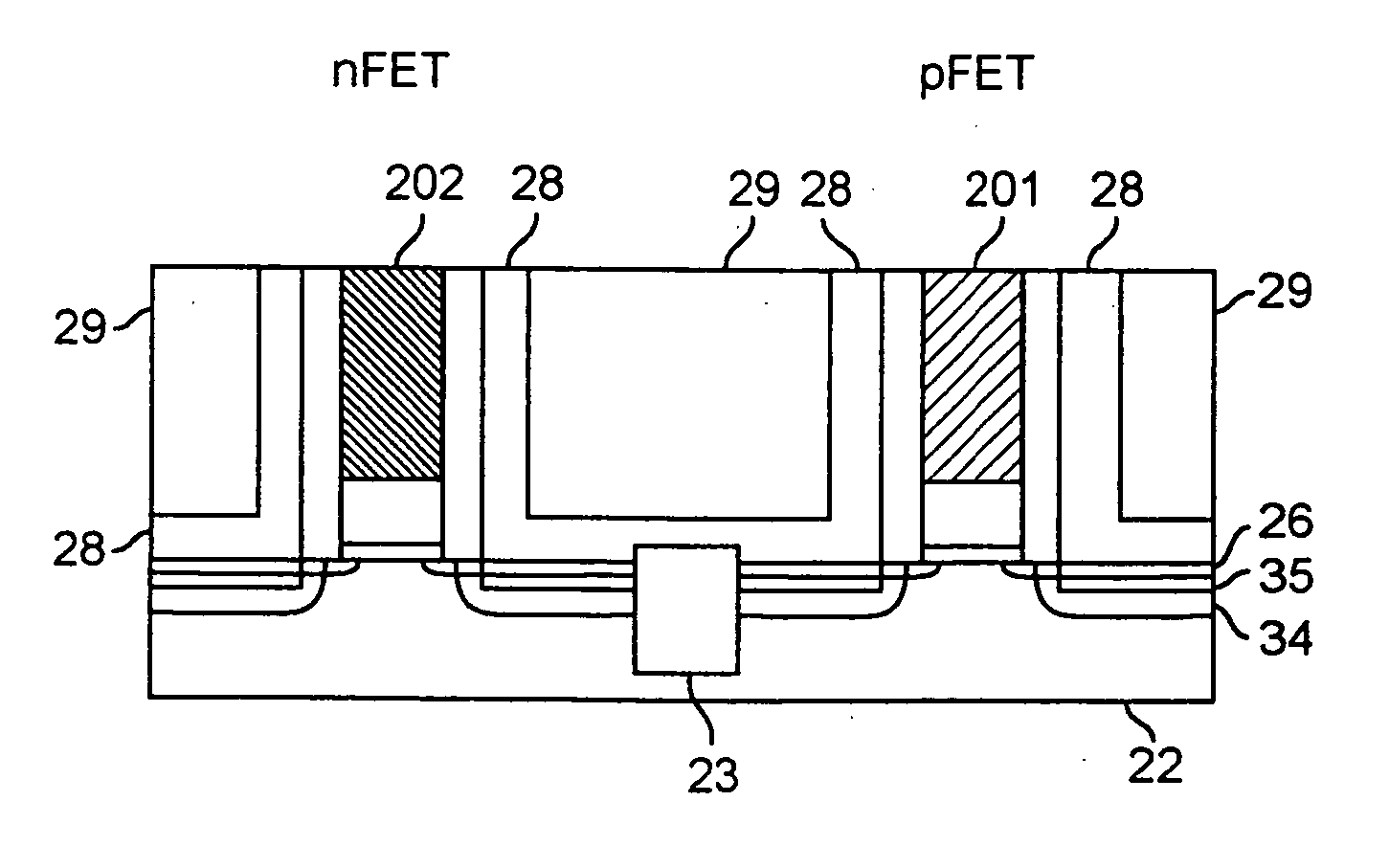
[0031] It should be appreciated in the course of the following discussion of FIGS. 1-12 that the embodiment which will be described is that which is expected to be the most advantageous in most applications and integrated circuits designs and thus allow the most complete appreciation and understanding of the invention to be conveyed. That is, the embodiment and variants thereof which will be described below will illustrate application of variable amounts of tensile and compressive stresses to respective adjacent transistors on a single chip and provide enhancement or other regulation of carrier mobility. However, the principles of the invention described in connection with this embodiment can also be applied to provide any desired amount of stress of either sign to adjacent transistors in any design and for any purpose.

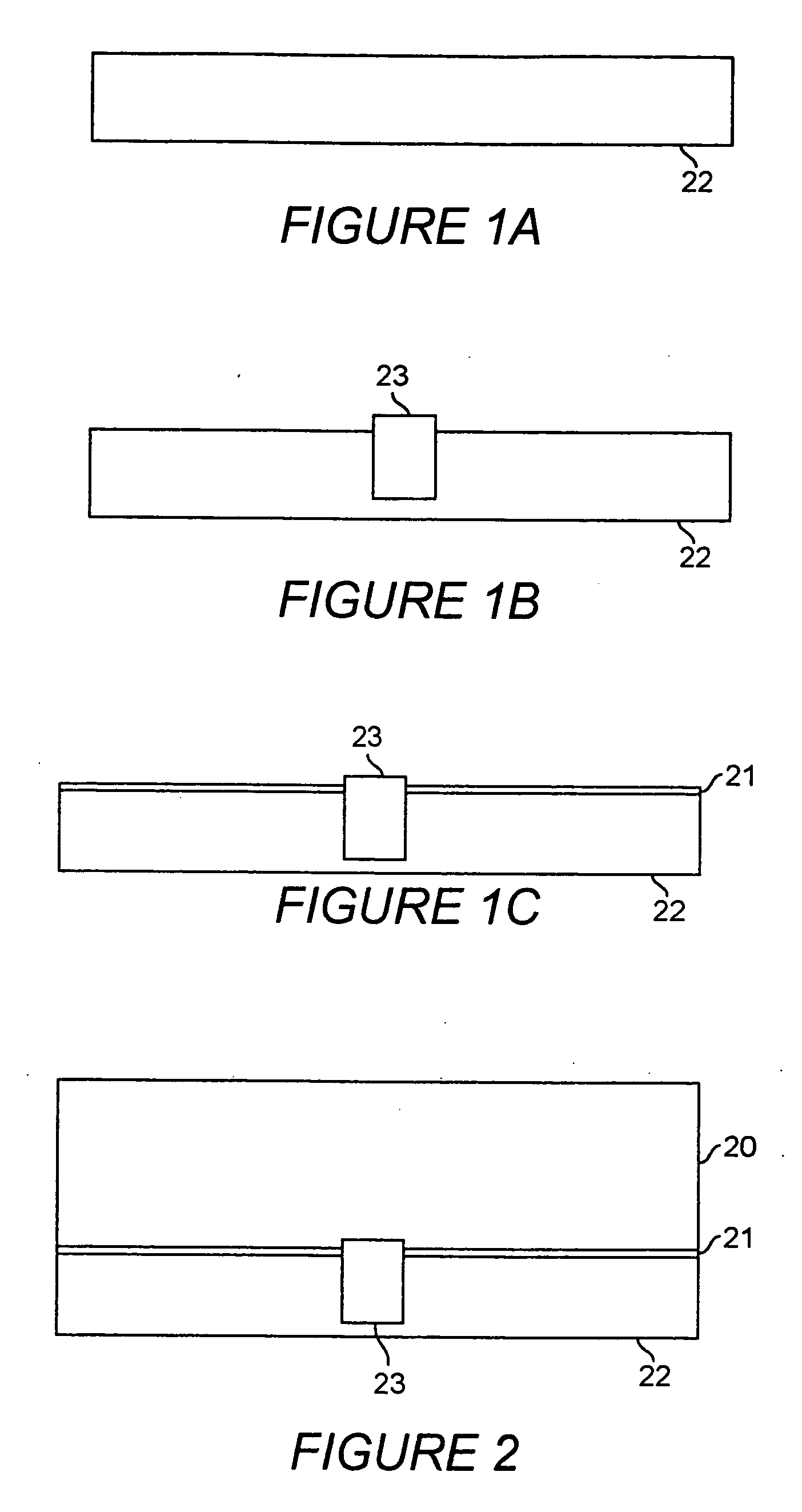
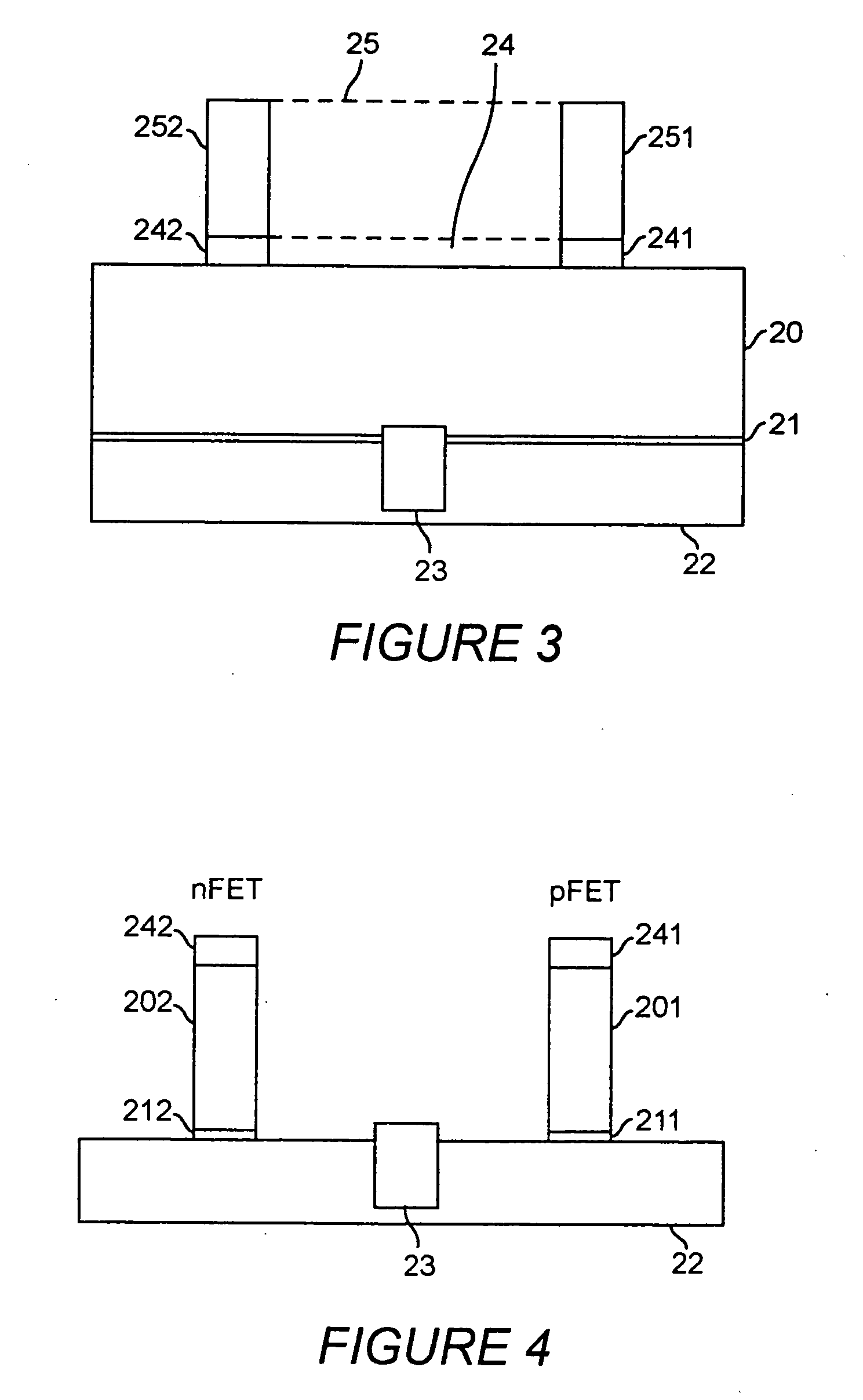
[0032] Referring now to the drawings, and more particularly to FIGS. 1a, 1b, and 1c, the first stages in making the preferred embodiment of the invention are shown i...


PUM

PropertyMeasurementUnit
carrier mobilityaaaaaaaaaa
tensile stressaaaaaaaaaa
compressive stressaaaaaaaaaa

Abstract

In producing complementary sets of metal-oxide-semiconductor (CMOS) field effect transistors, including nFET and pFET), carrier mobility is enhanced or otherwise regulated through the reacting the material of the gate electrode with a metal to produce a stressed alloy (preferably CoSi2, NiSi, or PdSi) within a transistor gate. In the case of both the nFET and pFET, the inherent stress of the respective alloy results in an opposite stress on the channel of respective transistor. By maintaining opposite stresses in the nFET and pFET alloys or silicides, both types of transistors on a single chip or substrate can achieve an enhanced carrier mobility, thereby improving the performance of CMOS devices and integrated circuits.

Description

BACKGROUND OF THE INVENTION [0001] 1. Field of the Invention [0002] The present invention generally relates to the manufacture of transistors for integrated circuits and, more particularly, to the production of complementary pairs of field effect transistors of enhanced performance at extremely small scale. [0003] 2. Description of the Prior Art [0004] Performance and economic factors of integrated circuit design and manufacture have caused the scale of elements (e.g. transistors, capacitors and the like) of integrated circuits to be drastically reduced in size and increased in proximity on a chip. That is, increased integration density and proximity of elements reduces the signal propagation path length and reduces signal propagation time and susceptibility to noise and increase of possible clock rates while the reduction in element size necessary for increased integration density increases the ratio of functionality which can be provided on a chip to the costs of production (e.g. ...

Claims


Application Information

Patent Timeline
Patent Type & Authority Applications(United States)
IPC IPC(8): H01L21/20H01L21/28H01L21/302H01L21/336H01L21/44H01L21/461H01L21/4763H01L21/8238H01L27/092H01L29/49H01L29/72H01L29/78H01L29/786H01L31/062
CPCH01L21/823807H01L21/823835H01L21/823842H01L29/785H01L29/66795H01L29/7845H01L29/4908
Inventor BELYANSKY, MICHAEL P.CHIDAMBARRAO, DURESETIDOKUMACI, OMER H.DORIS, BRUCE B.GLUSEHENKOV, OLEG
Owner GLOBALFOUNDRIES INC
Why Eureka
Try Eureka