Crosspoint structure semiconductor memory device, and manufacturing method thereof

a semiconductor memory and cross-section technology, applied in the direction of magnetic-field-controlled resistors, semiconductor devices, electrical devices, etc., can solve the problems of increasing power consumption, affecting the operation rate, and the memory cell area cannot be set smaller than 4fsup>2 /sup>in theory

Active Publication Date: 2005-12-15
XENOGENIC DEV LLC
View PDF13 Cites 65 Cited by
  • Summary
  • Abstract
  • Description
  • Claims
  • Application Information

AI Technical Summary

Benefits of technology

[0013] The present invention has been achieved in view of the conventional disadvantages. It is an object of the present invention to provide a semiconductor memory device that c

Problems solved by technology

The crosspoint structure memory cell has disadvantages such as a delay in operating rate caused by a parasitic current carried from unselected memory cells connected to the same bit line or word line as that to whic

Method used


Image

  • Crosspoint structure semiconductor memory device, and manufacturing method thereof
  • Crosspoint structure semiconductor memory device, and manufacturing method thereof
  • Crosspoint structure semiconductor memory device, and manufacturing method thereof

Examples


first embodiment

[0048] A first embodiment in which the method for manufacturing the semiconductor memory device according to the present invention (hereinafter, sometimes referred to as “the inventive method”) is applied to formation of upper electrode interconnectings and lower electrode interconnectings for crosspoint structure memory cells will be described.

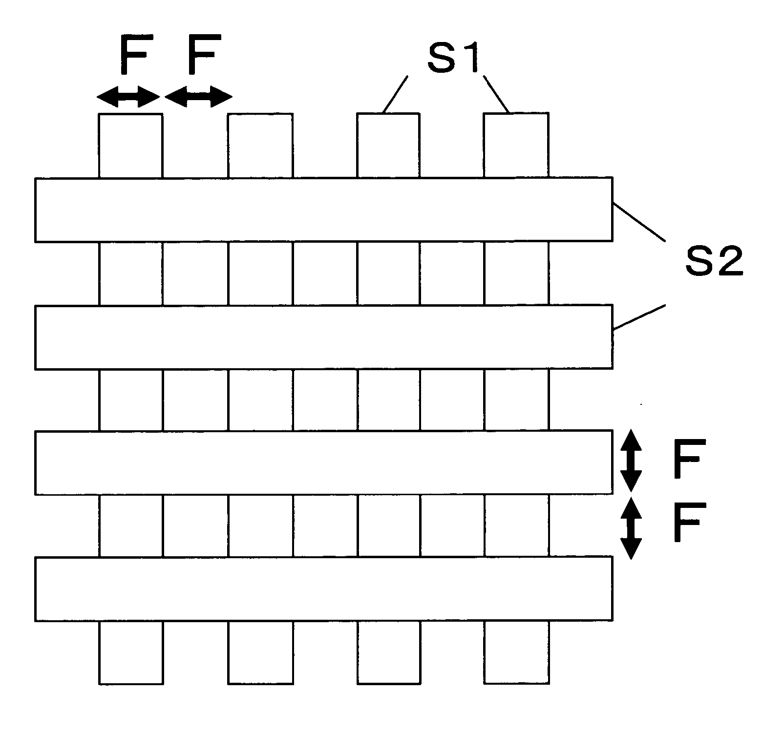
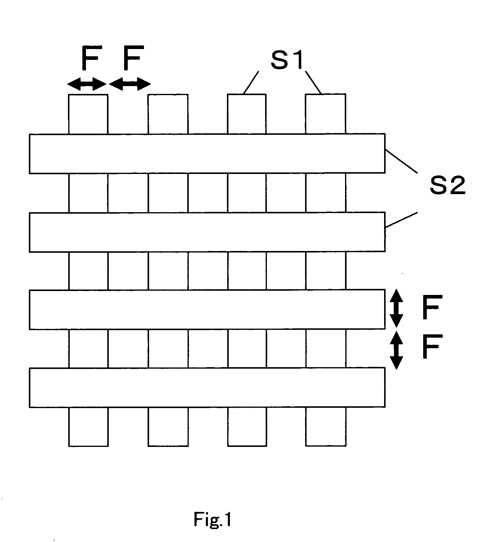
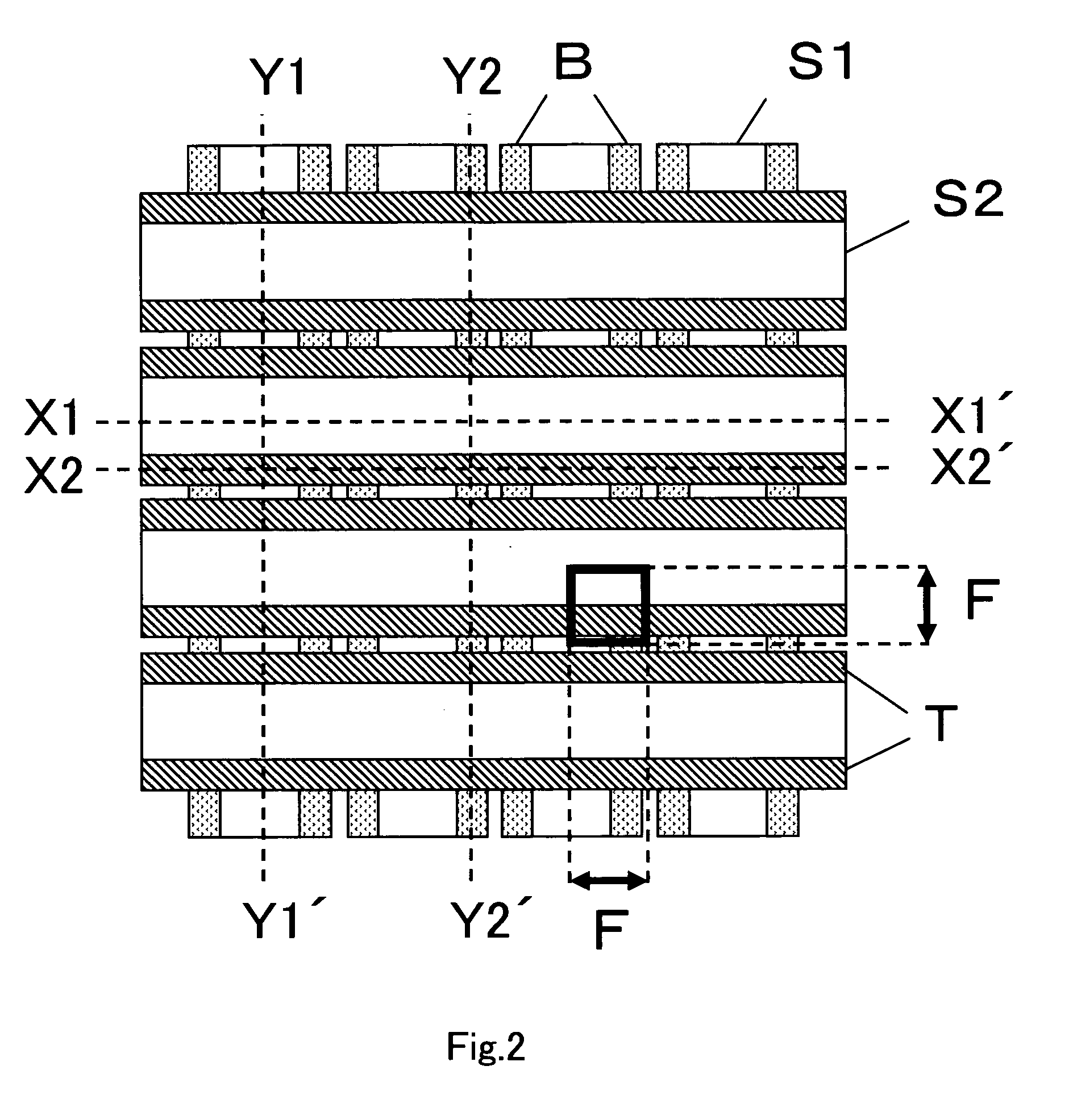
[0049]FIG. 1 is a layout plan view for forming memory cells and a memory cell array by the inventive method. In FIG. 1, reference symbol S1 denotes a region that defines a first insulation film pattern necessary to form lower electrode interconnectings B (see FIG. 2). Reference symbol S2 denotes a region that defines a second insulation film pattern necessary to form upper electrode interconnectings T (see FIG. 2).

[0050]FIG. 2 is a plan view that schematically shows the memory cell array of the semiconductor memory device manufactured by the inventive method based on the layout plan view of FIG. 1. In the first embodiment, the upper electro...

second embodiment

[0061] A second embodiment in which the inventive method is applied to formation of upper electrode interconnectings for crosspoint structure memory cells will be described.

[0062]FIG. 10 is a layout plan view for forming memory cells and a memory cell array by the inventive method. In FIG. 10, reference symbol R1 denotes a region that defines a interconnecting pattern of the lower electrode interconnectings B, and reference symbol S2 denotes a region that defines the second insulation film pattern necessary to form the upper electrode interconnectings T (see FIG. 11).

[0063]FIG. 11 is a plan view that schematically shows the memory cell array of the semiconductor memory device manufactured by the inventive method based on the layout plan view of FIG. 10. In the second embodiment, the upper electrode interconnectings T are formed along both sidewall surfaces of the second insulation film pattern S2 in a self-aligned manner.

[0064]FIGS. 12A-12D to FIGS. 16A-16D show the method accord...

third embodiment

[0072] A third embodiment in which the inventive method is applied to formation of lower electrode interconnectings for crosspoint structure memory cells will be described.

[0073]FIG. 17 is a layout plan view for forming memory cells and a memory cell array by the inventive method. In FIG. 17, reference symbol S1 denotes a region that defines a first insulation pattern necessary to form the lower electrode interconnectings B (see FIG. 18), and reference symbol R2 denotes a region that defines a interconnecting pattern of the upper electrode interconnectings T.

[0074]FIG. 18 is a plan view that schematically shows the memory cell array of the semiconductor memory device manufactured by the inventive method based on the layout plan view of FIG. 17. In the third embodiment, the lower electrode interconnectings B are formed along both sidewall surfaces of the first insulation film pattern S1 in a self-aligned manner.

[0075]FIGS. 19A-19D to FIGS. 21A-21D show the method according to the ...


PUM


Abstract

A crosspoint structure semiconductor memory device includes a plurality of upper electrode interconnectings extending in the same direction and a plurality of lower electrode interconnectings extending in a direction orthogonal to the extension direction of the upper electrode interconnectings. A storage material member that stores data is formed between the upper electrode interconnectings and the lower electrode interconnectings. At least either the upper electrode interconnectings or the lower electrode interconnectings are formed along sidewall surfaces of projections formed into stripes of an insulation film processed to have the projections.

Description

CROSS REFERENCE TO RELATED APPLICATTION [0001] This Nonprovisional application claims priority under 35 U.S.C. §119(a) on Patent Application No. 2004-172009 filed in Japan on Jun. 10, 2004, the entire contents of which are hereby incorporated by reference. BACKGROUND OF THE INVENTION [0002] 1. Field of the Invention [0003] The present invention relates to a crosspoint structure semiconductor memory device including a plurality of upper electrode interconnectings extending in the same direction and a plurality of lower electrode interconnectings extending in a direction orthogonal to the extension direction of the upper electrode interconnectings, and having a storage material member for storing data formed between the upper electrode interconnectings and the lower electrode interconnectings, and to a manufacturing method thereof. [0004] 2. Description of the Related Art [0005] Generally, in a semiconductor memory device such as a dynamic random access memory (DRAM), a NOR flash memo...

Claims


Application Information

Patent Timeline
IPC IPC(8): H01L21/3205H01L27/105H01L45/00H01L21/4763H01L27/22H01L27/24H01L43/08H01L21/768H01L21/8246H01L27/108
CPCH01L21/76838H01L27/222H01L45/04H01L45/1233H01L45/147H01L27/2463H10B61/00H10B63/80H10N70/20H10N70/8836H10N70/826
Inventor SHINMURA, NAOYUKI
Owner XENOGENIC DEV LLC
Why Eureka
Try Eureka