Method of manufacturing plasma display device
a technology of plasma display and manufacturing method, which is applied in the direction of manufacturing tools, identification means, instruments, etc., can solve the problems of metal chassis member and glass panel recycling, and the removal process is expensive in time and effor
- Summary
- Abstract
- Description
- Claims
- Application Information
AI Technical Summary
Problems solved by technology
Method used
Image

Examples
first exemplary embodiment
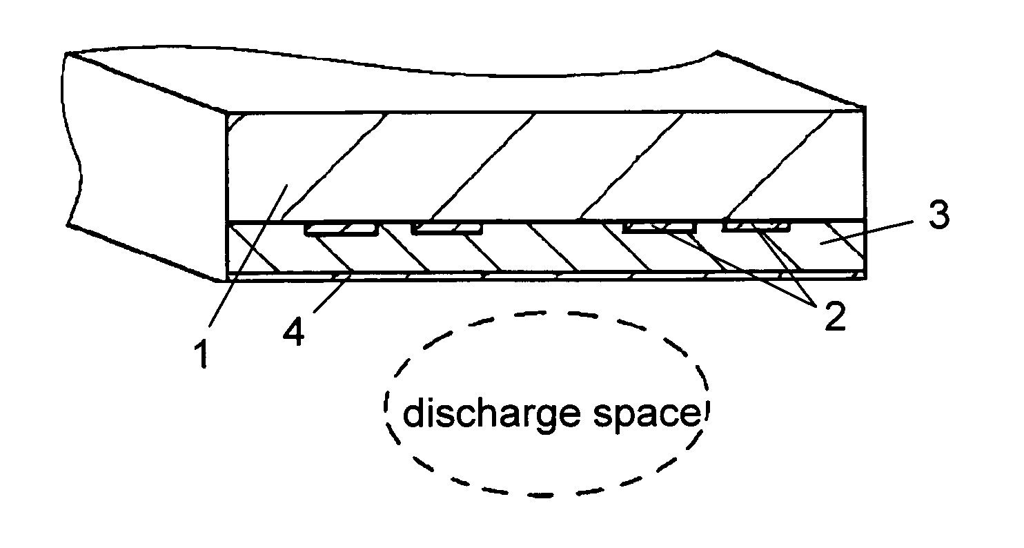
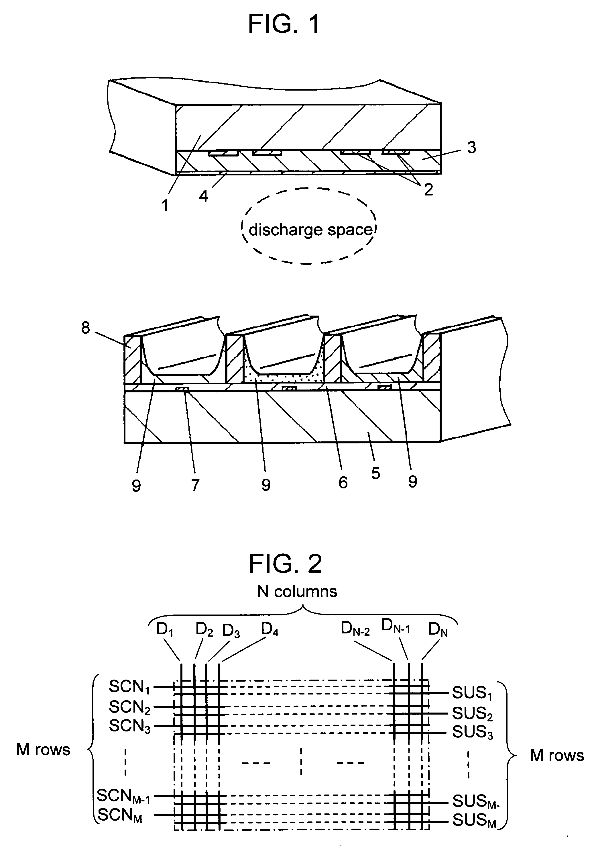
[0031] Referring to FIG. 1 through FIG. 8, the method of manufacturing a plasma display device of the invention will be described. The descriptions hereinafter will be given by way of example and without limitation.
[0032]FIG. 1 shows the structure of the panel of a plasma display device of a first exemplary embodiment of the present invention. On front-side transparent substrate 1 made of glass or the like, as shown in FIG. 1, a plurality of rows of display electrodes 2—made of pairs of the scan electrode and the sustain electrode—is formed in a stripe-shaped arrangement. The array of the electrodes is covered with dielectric layer 3, and over which, protecting film 4 is disposed.
[0033] On the other hand, on back-side substrate 5 confronting front-side substrate 1, a plurality of rows of data electrodes 7 is disposed so as to be orthogonal to the scan electrodes and sustain electrodes, i.e., display electrodes 2. Data electrodes 7 are covered with overcoat layer 6, and further on ...
second exemplary embodiment
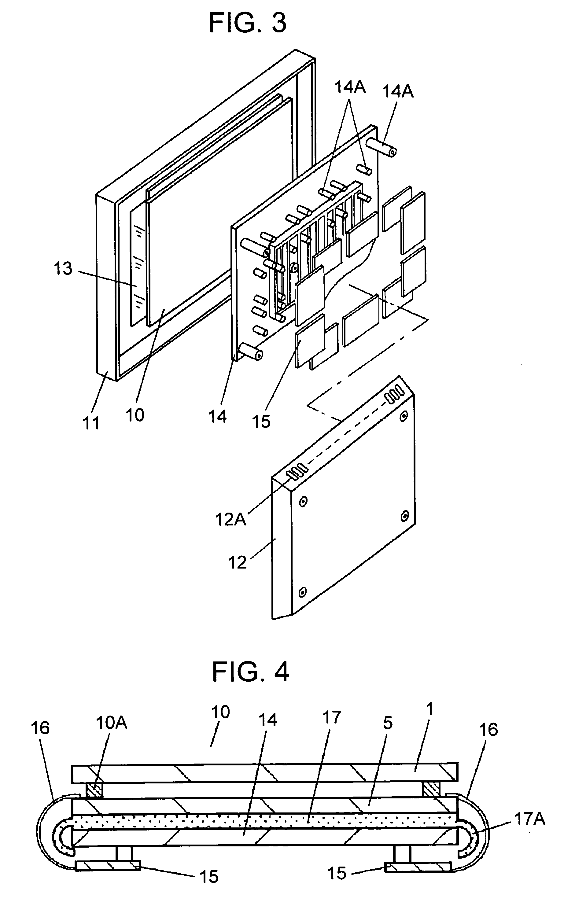
[0057] Next will be described the structure of the second exemplary embodiment. FIG. 9 is a section view taken along a line orthogonal to adhesive 17 applied to a plasma display panel of the second embodiment. FIG. 10 is a plan view showing patterns where the adhesive is applied.
[0058] Between panel 10 and chassis member 14, as shown in FIG. 9 and FIG. 10, adhesive 17 is provided in a rectangular shape where the width of the rectangular measured at remove-start point 17A—which is one end of the provided adhesive strip—gradually becomes smaller toward remove-end point 17B that is the other end of the strip of adhesive 17. Each strip is located on chassis member 14 so that remove-start point 17A and remove-end point 17B are alternately arranged with respect to the opposing sides of chassis member 14. That is, as shown in FIG. 10, the arrangement allows each strip to keep an interval substantially the same from the adjacent strip of adhesive 17. The adhesive strips at both ends of cha...
third exemplary embodiment
[0064] Next will be described the structure of the third exemplary embodiment. FIG. 12 is a section view taken along a line orthogonal to adhesive 17 applied to a plasma display panel of the third embodiment. FIG. 13 is a plan view of the chassis member, with adhesive 17 provided areas shown in crosshatch pattern.
[0065] A plurality of strips of adhesive 17 is, as shown in FIGS. 12 and 13, disposed at predetermined spaced intervals between panel 10 and chassis member 14. To properly keep the gap between panel 10 and chassis member 14, a plurality of spacers 21 is disposed between the strips of adhesive 17. Each spacer 21 is separately located pull-to-remove adhesive 21A in which beads 21B made of glass or resin are embedded.
[0066] Preferably, a strip of adhesive 17 should be provided so that a portion of the adhesive comes out from the bonded edges of panel 10 and chassis member 14 as an exposed tab with few millimeters to few centimeters in length. To separate panel 10 from chassi...
PUM
| Property | Measurement | Unit |
|---|---|---|
| transparency | aaaaa | aaaaa |
| thermal conductive | aaaaa | aaaaa |
| pressure | aaaaa | aaaaa |
Abstract
Description
Claims
Application Information
 - R&D
- Intellectual Property
- Life Sciences
- Materials
- Tech Scout
- Unparalleled Data Quality
- Higher Quality Content
- 60% Fewer Hallucinations
Browse by: Latest US Patents, China's latest patents, Technical Efficacy Thesaurus, Application Domain, Technology Topic, Popular Technical Reports.
© 2025 PatSnap. All rights reserved.Legal|Privacy policy|Modern Slavery Act Transparency Statement|Sitemap|About US| Contact US: help@patsnap.com