
Liquid crystal display device including sensing element

a technology of liquid crystal display and sensing element, which is applied in the direction of electric digital data processing, instruments, computing, etc., can solve the problems of high manufacturing cost, low productivity, and touch screen device provided by lcd devi

Inactive Publication Date: 2006-01-26
SAMSUNG DISPLAY CO LTD
View PDF3 Cites 255 Cited by
  • Summary
  • Abstract
  • Description
  • Claims
  • Application Information

AI Technical Summary

Benefits of technology

[0186] Having described the exemplary embodiments of the present invention and its advantages, it is noted that various changes, substitutions and alterations can be made herein without departing from the spirit and scope of the invention as defined by appended claims. Moreover, the use of the terms first, second, etc. does not denote any order of importance, but rather the terms first, second, etc. are used to distinguish one element from another. Furthermore, the use of the terms a, an, etc. does not denote a limitation of quantity, but rather denotes the presence of at least one of the referenced item.

Problems solved by technology

However, an LCD device provided with a touch screen panel has some defects including high manufacturing cost due to the cost of the touch screen panel, low productivity due to a step for attaching the touch screen panel to the LCD device, reduction of the luminance of the LCD device, increase of the thickness of the LCD device.
However, the characteristics of a photosensor depend on exterior environments such as strength of external light, strength of backlight lamps, temperature, etc., and thus there may be many errors on the light sensing caused by these factors such that the photosensor informs of the presence of a touch that is not actually present or it fails to inform the presence of an actual touch.
In addition, a photosensor in a pixel of a display device and signal lines for transmitting signals to the photosensor may decrease aperture ratio, thereby degrading the image quality.

Method used


Image

  • Liquid crystal display device including sensing element
  • Liquid crystal display device including sensing element
  • Liquid crystal display device including sensing element

Examples


Embodiment Construction

[0040] The present invention now will be described more fully hereinafter with reference to the accompanying drawings, in which preferred embodiments of the invention are shown.

[0041] In the drawings, the thickness of layers and regions are exaggerated for clarity. Like numerals refer to like elements throughout. It will be understood that when an element such as a layer, region or substrate is referred to as being “on” another element, it can be directly on the other element or intervening elements may also be present. In contrast, when an element is referred to as being “directly on” another element, there are no intervening elements present.

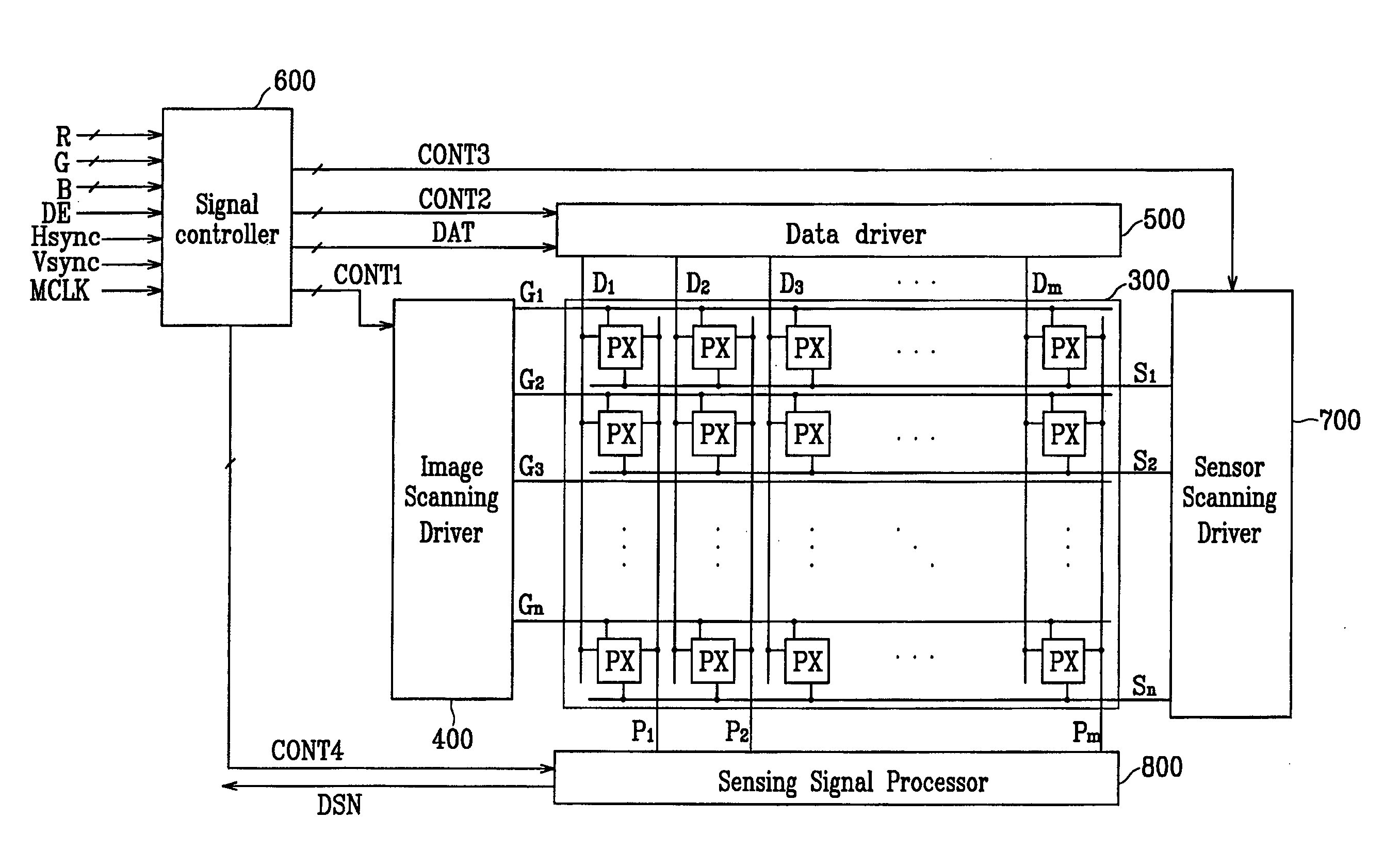
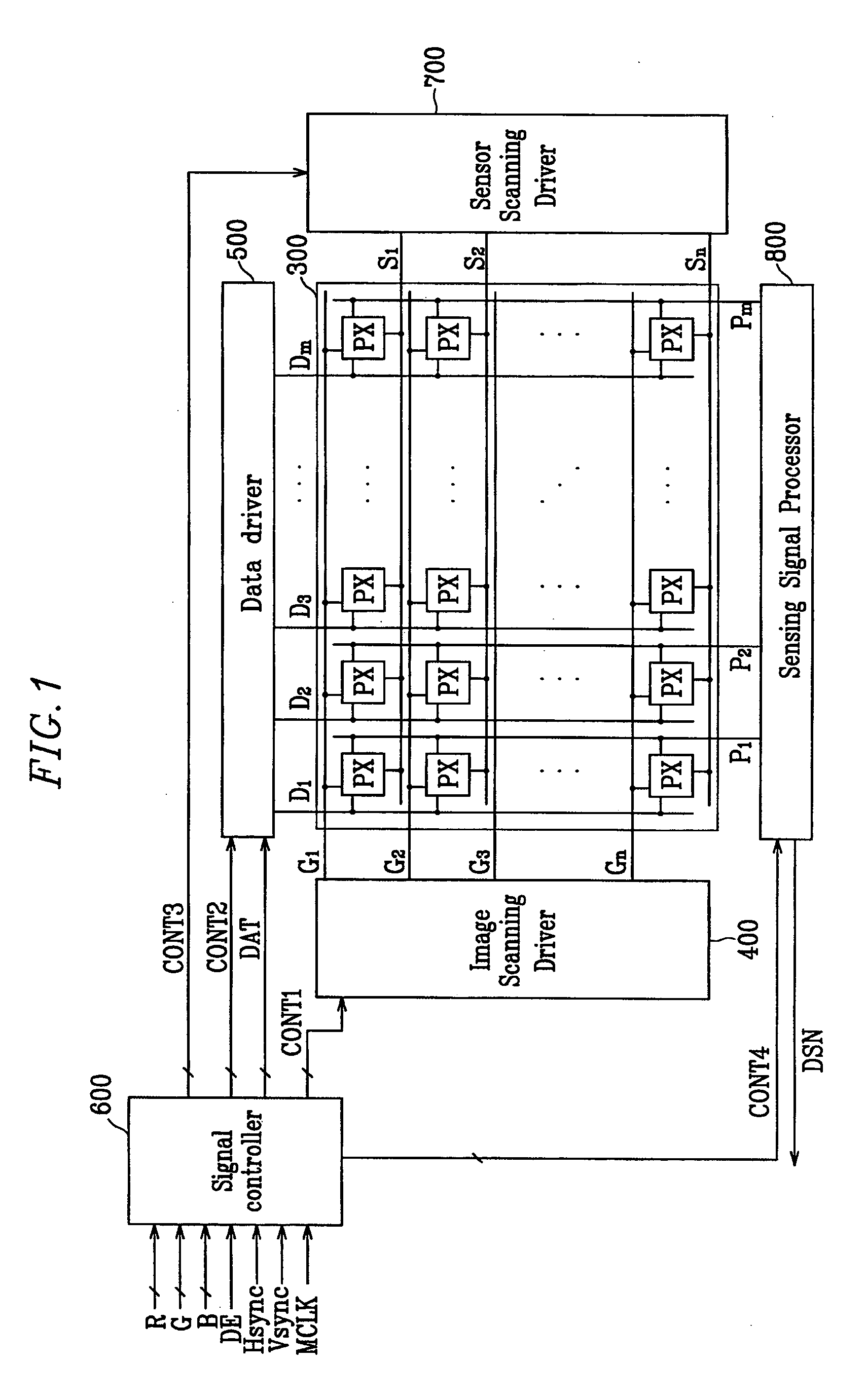
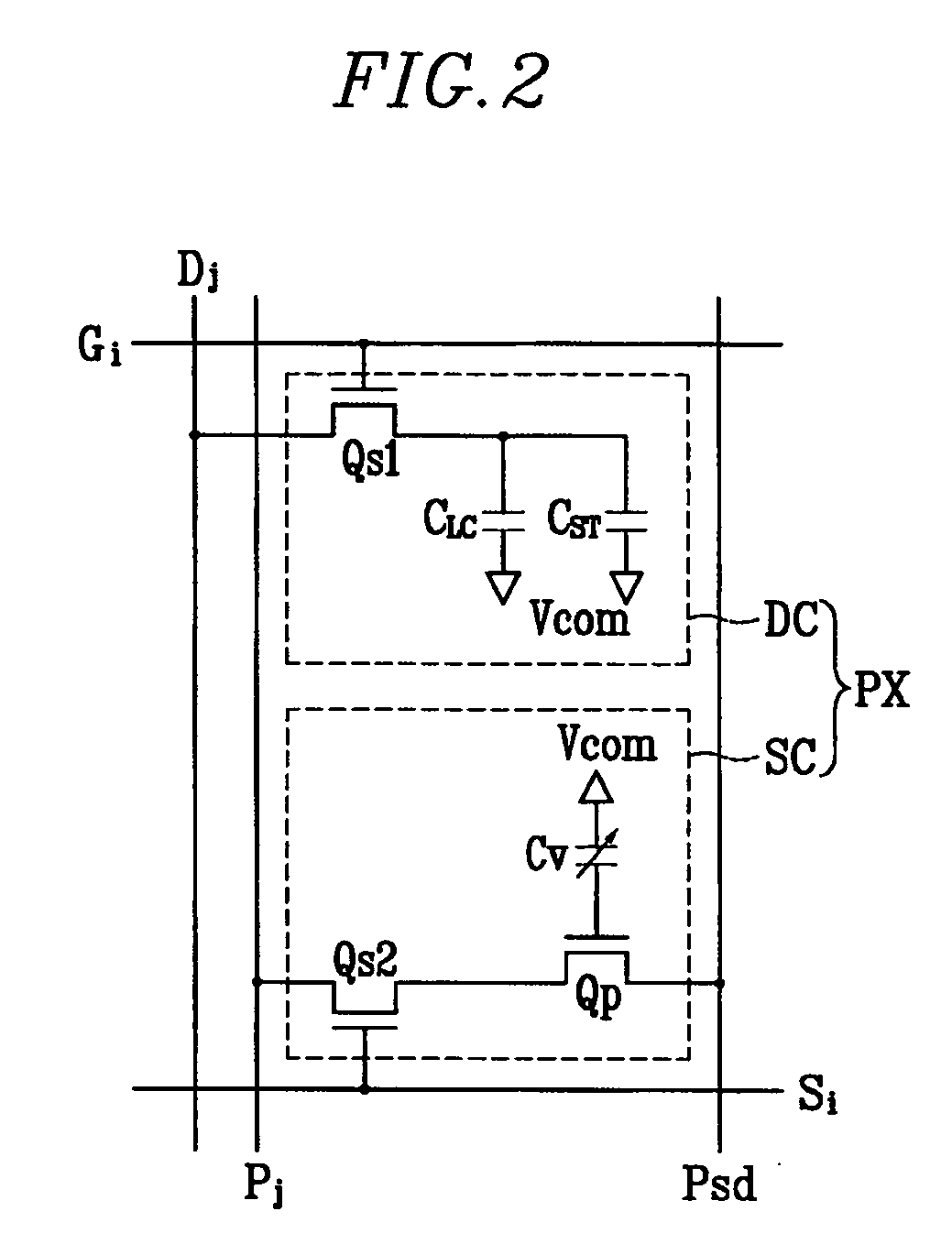
[0042] An exemplary embodiment of a liquid crystal display device according to the present invention will be described in detail with reference to FIGS. 1 and 2.

[0043]FIG. 1 is a block diagram of an exemplary embodiment of an LCD device according to the present invention, FIG. 2 is an equivalent circuit diagram of an exemplary embodiment of...


PUM


Abstract

A liquid crystal display includes a first panel, a second panel facing the first panel and spaced apart from the first panel, a liquid crystal layer disposed between the first panel and the second panel, a variable capacitor having a capacitance that varies by a touch and generating a control voltage that has a magnitude depending on the capacitance, and a sensing element disposed on the second panel and generating a sensing signal based on the control voltage.

Description

BACKGROUND OF THE INVENTION [0001] (a) Field of the Invention [0002] The present invention relates to a liquid crystal display device including a sensing element. [0003] (b) Description of Related Art [0004] A liquid crystal display (LCD) device includes a pair of panels provided with pixel electrodes and a common electrode and a liquid crystal layer with dielectric anisotropy interposed between the panels. The pixel electrodes are arranged in a matrix and connected to switching elements such as thin film transistors (TFTs) such that they receive image data voltages row by row. The common electrode covers entire surface of one of the two panels and it is supplied with a common voltage. A pixel electrode and corresponding portions of the common electrode, and corresponding portions of the liquid crystal layer form a liquid crystal capacitor as well as a switching element connected thereto constitute a basic element of a pixel. [0005] An LCD device generates electric fields by applyin...

Claims


Application Information

Patent Timeline
IPC IPC(8): G09G5/00
CPCG02F1/13338G09G2360/148G09G3/3648G06F3/0412G06F3/0447G06F3/042G06F2203/04106G02F1/133
Inventor LEE, JOO-HYUNGUH, KEE-HANPARK, JONG-WOUNGPARK, SANG-JIN
Owner SAMSUNG DISPLAY CO LTD
Learn More