Multichip module including a plurality of semiconductor chips, and printed circuit board including a plurality of components

a multi-chip module and printed circuit board technology, applied in the direction of semiconductor devices, semiconductor/solid-state device details, electrical apparatus, etc., can solve the problems of complex wiring arrangement connecting the semiconductor chips to one another, and achieve the effect of simple wiring arrangemen

Inactive Publication Date: 2006-03-23
INFINEON TECH AG
View PDF26 Cites 34 Cited by
  • Summary
  • Abstract
  • Description
  • Claims
  • Application Information

AI Technical Summary

Benefits of technology

[0004] It is an object of the invention to provide a multichip module that includes a plurality of semiconductor chips and a simple wiring arrangement.

Problems solved by technology

The wiring arrangement connecting the semiconductor chips to one another is often very complex and very cost intensive.

Method used


Image

  • Multichip module including a plurality of semiconductor chips, and printed circuit board including a plurality of components
  • Multichip module including a plurality of semiconductor chips, and printed circuit board including a plurality of components
  • Multichip module including a plurality of semiconductor chips, and printed circuit board including a plurality of components

Examples


Embodiment Construction

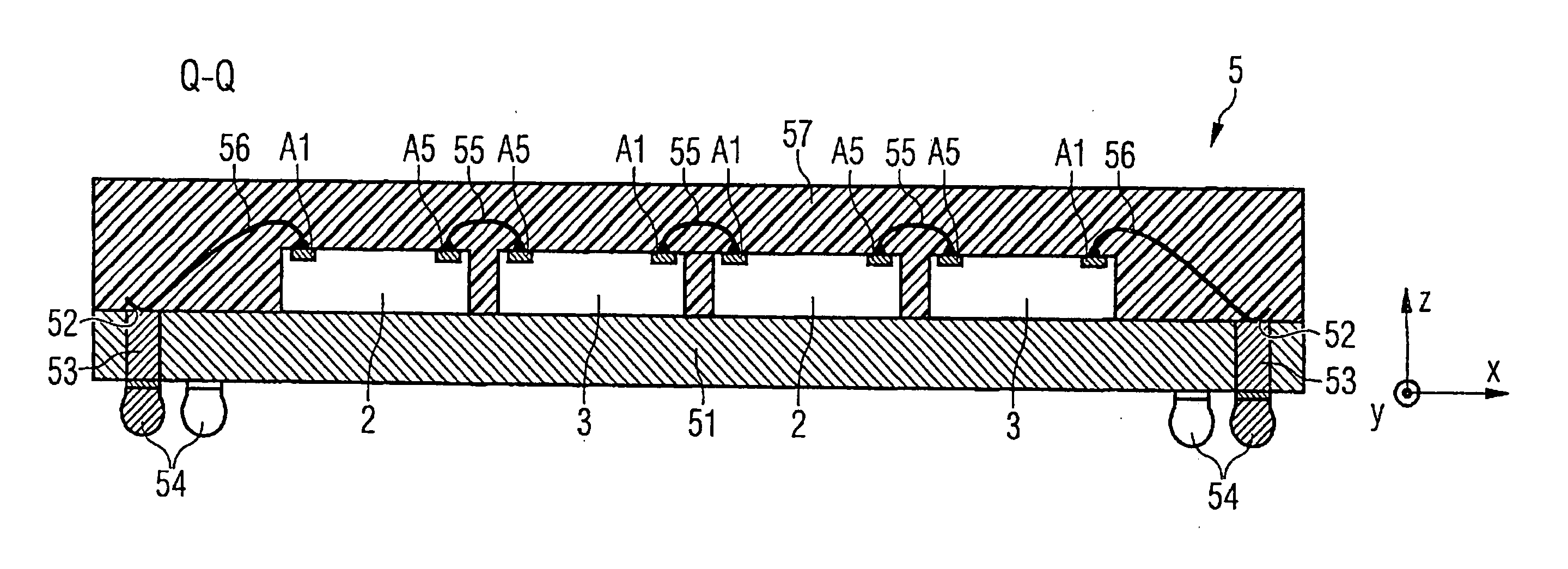
[0060]FIG. 1 shows a plan view of a semiconductor chip arrangement 1 with semiconductor chips arranged in rows and in columns, where the active top sides of the semiconductor chips are shown.

[0061] The following terms “next to one another”, “behind one another”, “above one another” and “on one another”, as used in relation to FIGS. 1 and 2, are standardized according to an axis system with the coordinate axes x, y and z as shown next to the semiconductor chip arrangement 1 in FIG. 1. In this context, the term “next to one another” is used with reference to the x axis, the term “behind one another” is used with reference to the y axis and the term “above one another” and “on one another” are used with reference to the z axis.

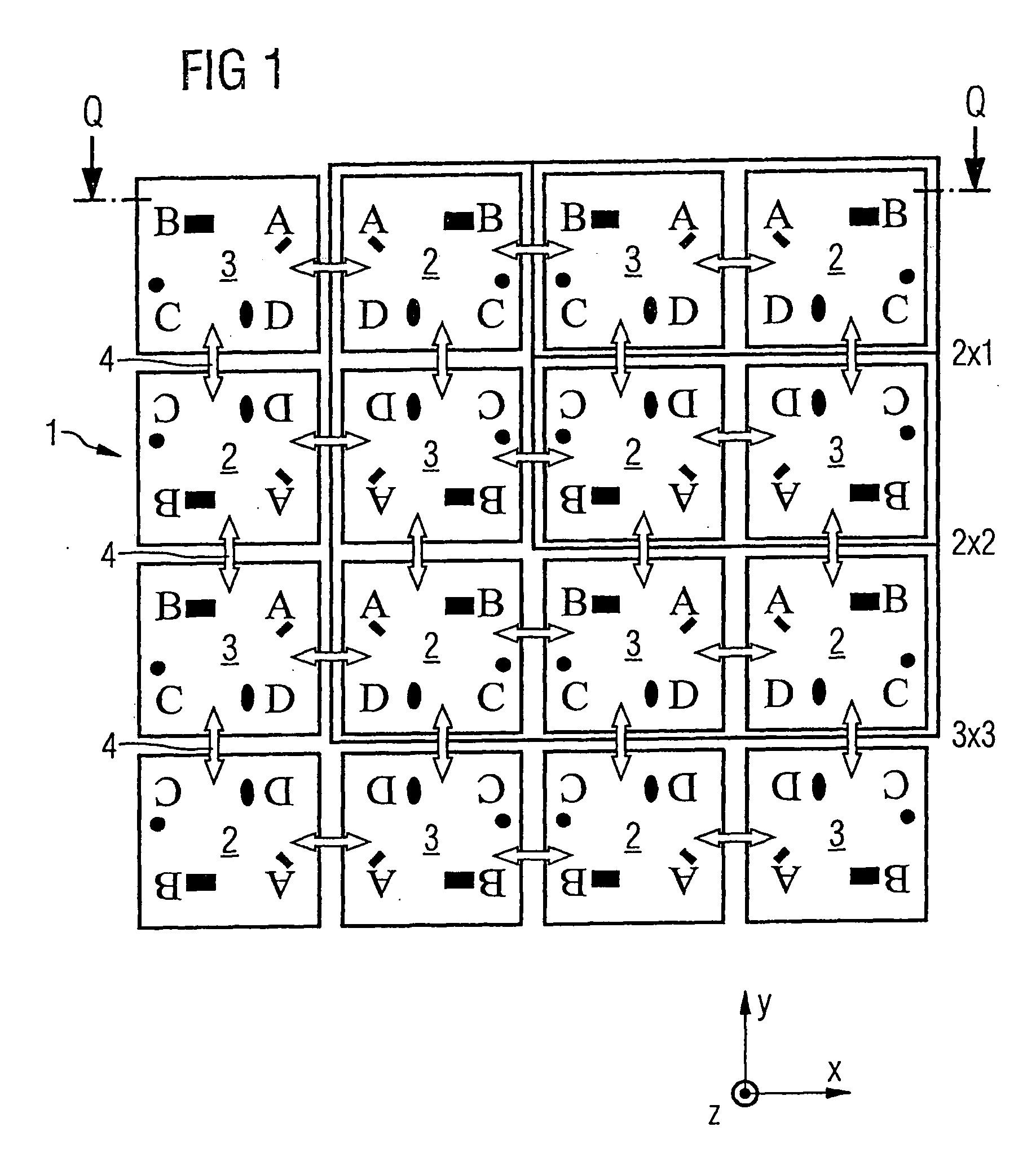
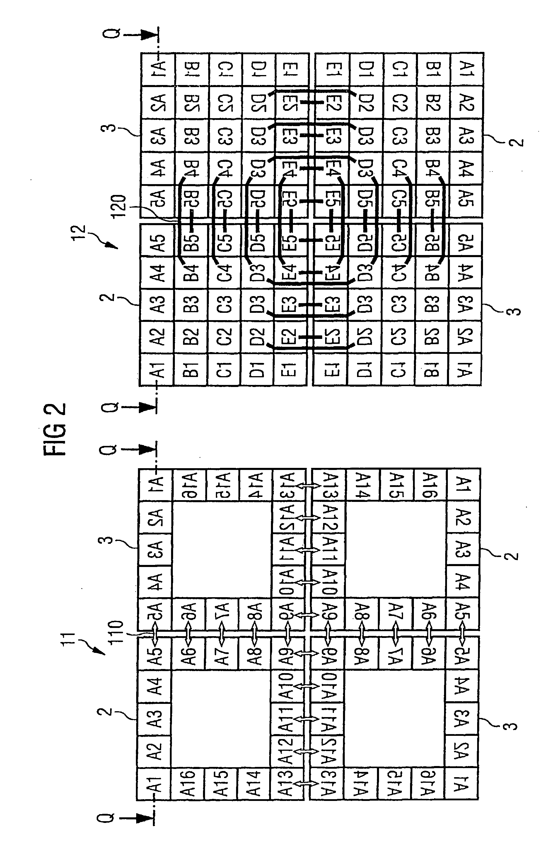
[0062] The semiconductor chip arrangement 1 of FIG. 1 is designed as a square 4×4 matrix. However, and as also shown in FIG. 1, it is noted that semiconductor chip arrangements based on the invention may also be in the form of 2×1, 2×2 or 3×3 matrices or in the...


PUM


Abstract

A multichip module includes at least one first semiconductor chip and at least one second semiconductor chip. The semiconductor chips are arranged in coplanar fashion on or in a support medium and respectively include matching components and contact areas arranged on their active top sides. At least one second semiconductor chip includes an arrangement of contact areas which is mirror-inverted in relation to a first semiconductor chip. At least one first semiconductor chip and at least one second semiconductor chip are arranged next to and/or behind one another (i.e., adjacent to one another) such that those of their edges which respectively have a matching arrangement of contact areas are opposite one another. Wiring arrangements extend between respectively opposite contact areas and between contact areas at the outer edges of the semiconductor chips and external contacts.

Description

CROSS-REFERENCE TO RELATED APPLICATIONS [0001] This application is a continuation of PCT / DE2004 / 000750, filed, Apr. 8, 2004, and titled “Multichip Module Comprising A Plurality Of Semiconductor Chips, And Printed Circuit Board Comprising A Plurality Of Components,” which claims priority under 35 U.S.C. §119 to German Application No. DE 103 17 018.9, filed on Apr. 11, 2003, and titled “Multichip Module Comprising A Plurality Of Semiconductor Chips, And Printed Circuit Board Comprising A Plurality Of Components,” the entire contents of each are hereby incorporated by reference.FIELD OF THE INVENTION [0002] The invention relates to a multichip module including a plurality of semiconductor chips and also to a printed circuit board including a plurality of components. BACKGROUND [0003] Electronic devices are known which have a plurality of semiconductor chips arranged next to one another on a mounting substrate. In this arrangement, these semiconductor chips have contact areas which are ...

Claims


Application Information

Patent Timeline
Patent Type & Authority Applications(United States)
IPC IPC(8): H01L23/02H01L21/60H01L23/538H01L25/065
CPCH01L23/5389H01L2224/24137H01L24/85H01L24/96H01L25/0655H01L2224/04105H01L2224/20H01L2224/211H01L2224/48091H01L2224/48137H01L2224/48227H01L2224/48464H01L2224/85H01L2924/01004H01L2924/01006H01L2924/0101H01L2924/01013H01L2924/01014H01L2924/01028H01L2924/01032H01L2924/01039H01L2924/01052H01L2924/01061H01L2924/01075H01L2924/01078H01L2924/01079H01L2924/01082H01L2924/14H01L2924/15311H01L2924/1532H01L24/19H01L2924/07802H01L2224/0401H01L2224/16225H01L24/48H01L2224/16227H01L2924/00014H01L2924/01005H01L2924/01019H01L2924/01024H01L2924/01033H01L2924/01068H01L2924/01087H01L2924/014H01L2224/73267H01L2224/32245H01L2224/32225H01L2224/48465H01L24/24H01L2224/78H01L2924/00H01L2224/12105H01L2224/451H01L24/45H01L2924/181H01L2924/00012
Inventor MEYER-BERG, GEORG
Owner INFINEON TECH AG
Why Eureka
Try Eureka