Face-to-face bonded I/O circuit die and functional logic circuit die system

a functional logic and circuit die technology, applied in the field of integrated circuit technology, can solve the problems of unneeded gates, unsatisfactory solutions for i/o problems, and customers may need a significant amount of i/o and not many gates,

Active Publication Date: 2006-04-06
MICROSEMI SOC
View PDF16 Cites 218 Cited by
  • Summary
  • Abstract
  • Description
  • Claims
  • Application Information

AI Technical Summary

Problems solved by technology

A secondary cost issue is that often customers may need a significant amount of I / O and not many gates.
Another problem is that some manufacturers envision creating a number of system-on-a-chip (SOC) integrated circuits and derivatives that employ FPGA and other programmable logic technology.
In addition, the number of FPGA gates needed for each set of peripherals will be customer dependent, again creating a situation where the customer is paying for un-needed gates.
The industry has not come up with a good solution for the I / O problem to date.
Therefore, with prior art systems, there is often a trade-off between ESD protection and the number of available I / O circuits.
This solution however requires flip-chip packaging.
None of these variations are employing 3D packaging to solve the above-described I / O problem.

Method used


Image

  • Face-to-face bonded I/O circuit die and functional logic circuit die system
  • Face-to-face bonded I/O circuit die and functional logic circuit die system
  • Face-to-face bonded I/O circuit die and functional logic circuit die system

Examples


Embodiment Construction

[0014] Those of ordinary skill in the art will realize that the following description of the present invention is illustrative only and not in any way limiting. Other embodiments of the invention will readily suggest themselves to such skilled persons.

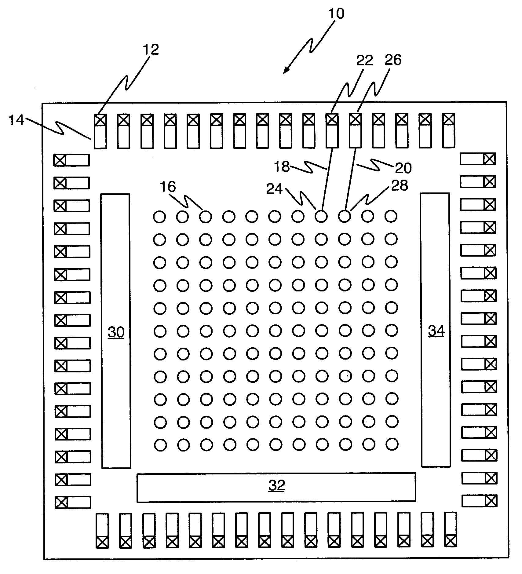
[0015] The I / O circuit portion of an FPGA can be manufactured on mature processes because, among other reasons, a system designer requires higher voltage board signaling than that needed for the FPGA core. That is, while the FPGA may operate at one voltage such as 1.5 volts, the I / O circuits may need to be able to operate at other voltages such as, for example, 3-5 volts, to handle various customer applications.

[0016] Wafer prices for circuits manufactured using such mature processes are typically steeply discounted relative to leading-edge processes. For example, at a time when 90 nm feature size is the leading edge of FPGA processes, an I / O chip for a 90 nm FPGA device may be produced using a 180 nm process. Mature processes can su...


PUM


Abstract

An integrated circuit system includes a first set of integrated circuit dice each member of the set having a different configuration of input / output circuits disposed thereon and a second set of integrated circuit dice each having different logical function circuits disposed thereon. Each member of the first and second sets of integrated circuit dice include an array of face-to-face bonding pads disposed thereon that mate with the array of face-to-face bonding pads of each member of the other set.

Description

BACKGROUND [0001] 1. Field of the Invention [0002] The present invention relates to integrated circuit technology. More particularly, the present invention relates to an integrated circuit system including mating sets of face-to-face integrated circuit dice. [0003] 2. The Prior Art [0004] As process geometries scale, the portion of the area of digital-logic function integrated circuits such as field-programmable-gate-array (FPGA) integrated circuits and mixed digital and analog function integrated circuits that must be devoted to input / output circuits (I / O) represents an increasing percentage of the die area relative to logic gates. A secondary cost issue is that often customers may need a significant amount of I / O and not many gates. Presently, such customers end up paying for un-needed gates in order to obtain needed I / O. The reverse is true as well. This represents an opportunity to deliver a more cost-effective product to customers. [0005] Another problem is that some manufactur...

Claims


Application Information

Patent Timeline
Patent Type & Authority Applications(United States)
IPC IPC(8): H01L23/48
CPCH01L25/18H01L2224/16145H01L2225/0651H01L2225/06513H03K19/17732H03K19/17744H03K19/17796H01L2224/05573H01L2924/00014H01L2224/0554H01L24/06H01L2224/06136H01L24/05H01L2224/05599H01L2224/0555H01L2224/0556H01L2224/05568
Inventor SPEERS, THEODORE
Owner MICROSEMI SOC
Why Eureka
Try Eureka